Home > Press > FEI Completes Multiple System Installation at New Materials Ageing Institute Research Center in France
 |
Abstract:
World's leading nuclear operators collaborate in an effort to extend the lifetime of power plants.
FEI Completes Multiple System Installation at New Materials Ageing Institute Research Center in France
Hillsboro, OR | Posted on March 3rd, 2010FEI Company (NASDAQ: FEIC), a leading diversified scientific instruments company providing electron and ion-beam microscopes and tools for nanoscale applications across many industries, announces the completion of a multiple system installation at the Materials Ageing Institute (MAI) in France, a utility-oriented research center financed by Electricit� de France (EDF), the Tokyo Electric Power Company (TEPCO), the Kansai Electric Power Company (KEPCO) and the US Electric Power Research Institute (EPRI).
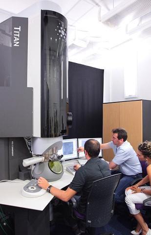
The MAI microscopy laboratory has now commissioned its new FEI Titan� Scanning Transmission Electron Microscope (S/TEM) microscope, the most powerful commercially-available microscope in the world. The Titan joins the MAI's FEI Tecnai� S/TEM, Helios DualBeam� and Quanta� 600 Field Emission Gun (FEG) in one of the world's premier microscopy facilities, where they will be used to study the ageing of materials to improve the reliability and safety, and extend the lifetimes, of nuclear and non-nuclear power plants.
"The Titan's ability to resolve atomic detail is absolutely essential to our work," said Laurent Legras, head of the MAI MET laboratory. "Many of the earliest and most fundamental steps of the ageing process are only visible at the atomic level. With the Titan, we can compare real materials to our computer simulations to verify our understanding of the ageing mechanisms and processes specific to nuclear power generation. We can also study chemical bonding, oxidation, corrosion, and other processes that apply more broadly to most types of power generation. This combination of operational experience, experimental knowledge, and computer modeling of coupled processes then allows us to anticipate ageing and increase the durability of the materials, components and structures used in power plants."
Tony Edwards, FEI's senior vice president, market divisions, said, "FEI shares a long history with EDF, the French nuclear giant that played a key role in the development and construction of the MAI. This is an outstanding example of how imaging and characterization at the atomic scale can enable advances in energy technologies. The ability to characterize, and even manipulate, materials at atomic scale provides critical insights into valuable new technologies and permits continual improvements to those already in use. We are pleased that the Titan and other FEI microscopes are now generating crucial data for this important work."
The Tecnai S/TEM is used for routine investigations of structure and composition. The Helios DualBeam combines scanning electron microscope (SEM) imaging and focused ion beam (FIB) milling to allow high-resolution imaging and analysis of three-dimensional structures and subsurface defects. The Quanta 600 FEG permits SEM examination of samples under a wide variety of vacuum and environmental conditions, including dynamic observations of oxidation, corrosion, and other chemical and physical ageing processes.
Please see www.fei.com or http:/themai.org for more information about FEI or the MAI.
FEI Safe Harbor Statement
This news release contains forward-looking statements that include statements regarding the performance capabilities and benefits of the Titan S/TEM. Factors that could affect these forward-looking statements include but are not limited to failure of the product or technology to perform as expected and achieve anticipated results, unexpected technology problems and our ability to manufacture, ship and deliver the tools as expected. Please also refer to our Form 10-K, Forms 10-Q, Forms 8-K and other filings with the U.S. Securities and Exchange Commission for additional information on these factors and other factors that could cause actual results to differ materially from the forward-looking statements. FEI assumes no duty to update forward-looking statements.
####
About FEI
FEI (Nasdaq: FEIC) is a leading diversified scientific instruments company. It is a premier provider of electron and ion-beam microscopes and tools for nanoscale applications across many industries: industrial and academic materials research, life sciences, semiconductors, data storage, natural resources and more. With a 60-year history of technological innovation and leadership, FEI has set the performance standard in transmission electron microscopes (TEM), scanning electron microscopes (SEM) and DualBeams�, which combine a SEM with a focused ion beam (FIB). FEI�s imaging systems provide 3D characterization, analysis and modification/prototyping with resolutions down to the sub-�ngstr�m (one-tenth of a nanometer) level. FEI�s NanoPorts in North America, Europe and Asia provide centers of technical excellence where its world-class community of customers and specialists collaborate. FEI has approximately 1800 employees and sales and service operations in more than 50 countries around the world. More information can be found at: www.fei.com.
For more information, please click here
Contacts:
Sandy Fewkes, Principal (media contact)
MindWrite Communications, Inc
+1 408 224 4024
FEI Company
Fletcher Chamberlin (investors and analysts)
Investor Relations
+1 503 726 7710
Copyright © FEI
If you have a comment, please Contact us.Issuers of news releases, not 7th Wave, Inc. or Nanotechnology Now, are solely responsible for the accuracy of the content.
Bookmark:


| Related News Press |
News and information
![]() Simulating magnetization in a Heisenberg quantum spin chain April 5th, 2024
Simulating magnetization in a Heisenberg quantum spin chain April 5th, 2024
![]() NRL charters Navy�s quantum inertial navigation path to reduce drift April 5th, 2024
NRL charters Navy�s quantum inertial navigation path to reduce drift April 5th, 2024
![]() Discovery points path to flash-like memory for storing qubits: Rice find could hasten development of nonvolatile quantum memory April 5th, 2024
Discovery points path to flash-like memory for storing qubits: Rice find could hasten development of nonvolatile quantum memory April 5th, 2024
Announcements
![]() NRL charters Navy�s quantum inertial navigation path to reduce drift April 5th, 2024
NRL charters Navy�s quantum inertial navigation path to reduce drift April 5th, 2024
![]() Discovery points path to flash-like memory for storing qubits: Rice find could hasten development of nonvolatile quantum memory April 5th, 2024
Discovery points path to flash-like memory for storing qubits: Rice find could hasten development of nonvolatile quantum memory April 5th, 2024
Tools
![]() Ferroelectrically modulate the Fermi level of graphene oxide to enhance SERS response November 3rd, 2023
Ferroelectrically modulate the Fermi level of graphene oxide to enhance SERS response November 3rd, 2023
![]() The USTC realizes In situ electron paramagnetic resonance spectroscopy using single nanodiamond sensors November 3rd, 2023
The USTC realizes In situ electron paramagnetic resonance spectroscopy using single nanodiamond sensors November 3rd, 2023
Energy
![]() Development of zinc oxide nanopagoda array photoelectrode: photoelectrochemical water-splitting hydrogen production January 12th, 2024
Development of zinc oxide nanopagoda array photoelectrode: photoelectrochemical water-splitting hydrogen production January 12th, 2024
![]() Shedding light on unique conduction mechanisms in a new type of perovskite oxide November 17th, 2023
Shedding light on unique conduction mechanisms in a new type of perovskite oxide November 17th, 2023
![]() Inverted perovskite solar cell breaks 25% efficiency record: Researchers improve cell efficiency using a combination of molecules to address different November 17th, 2023
Inverted perovskite solar cell breaks 25% efficiency record: Researchers improve cell efficiency using a combination of molecules to address different November 17th, 2023
![]() The efficient perovskite cells with a structured anti-reflective layer � another step towards commercialization on a wider scale October 6th, 2023
The efficient perovskite cells with a structured anti-reflective layer � another step towards commercialization on a wider scale October 6th, 2023
New-Contracts/Sales/Customers
![]() Bruker Light-Sheet Microscopes at Major Comprehensive Cancer Center: New Advanced Imaging Center Powered by Two MuVi and LCS SPIM Microscopes March 25th, 2021
Bruker Light-Sheet Microscopes at Major Comprehensive Cancer Center: New Advanced Imaging Center Powered by Two MuVi and LCS SPIM Microscopes March 25th, 2021
![]() Arrowhead Pharmaceuticals Announces Closing of Agreement with Takeda November 27th, 2020
Arrowhead Pharmaceuticals Announces Closing of Agreement with Takeda November 27th, 2020
![]() Veeco Announces Aledia Order of 300mm MOCVD Equipment for microLED Displays: Propel� Platform First 300mm System with EFEM Designed for Advanced Display Applications October 20th, 2020
Veeco Announces Aledia Order of 300mm MOCVD Equipment for microLED Displays: Propel� Platform First 300mm System with EFEM Designed for Advanced Display Applications October 20th, 2020
![]() GREENWAVES TECHNOLOGIES Announces Next Generation GAP9 Hearables Platform Using GLOBALFOUNDRIES 22FDX Solution October 16th, 2020
GREENWAVES TECHNOLOGIES Announces Next Generation GAP9 Hearables Platform Using GLOBALFOUNDRIES 22FDX Solution October 16th, 2020
|
|
||
|
|
||
| The latest news from around the world, FREE | ||
|
|
||
|
|
||
| Premium Products | ||
|
|
||
|
Only the news you want to read!
Learn More |
||
|
|
||
|
Full-service, expert consulting
Learn More |
||
|
|
||