Home > Press > Rice researchers make graphene hybrid
 |
Abstract:
One-atom-thick sheet offers new microelectronic possibilities
Rice researchers make graphene hybrid
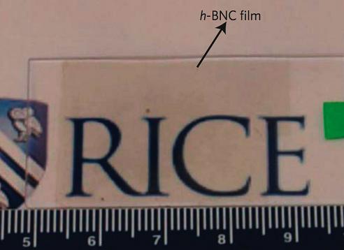
Houston, TX | Posted on March 3rd, 2010Rice University researchers have found a way to stitch graphene and hexagonal boron nitride (h-BN) into a two-dimensional quilt that offers new paths of exploration for materials scientists.
The technique has implications for application of graphene materials in microelectronics that scale well below the limitations of silicon determined by Moore's Law.
New research from the lab of Pulickel Ajayan, Rice's Benjamin M. and Mary Greenwood Anderson Professor in Mechanical Engineering and Materials Science and of chemistry, demonstrates a way to achieve fine control in the creation of such hybrid, 2-D structures.
Layers of h-BN a single atom thick have the same lattice structure as graphene, but electrically the materials are at opposite ends of the spectrum: h-BN is an insulator, whereas graphene, the single-atom-layer form of carbon, is highly conductive. The ability to assemble them into a single lattice could lead to a rich variety of 2-D structures with electric properties ranging from metallic conductor to semiconductor to insulator.
Because graphene is a conductor and h-BN is an insulator, the proportion of one to the other determines how well this new material conducts electrons. Lijie Ci and Li Song, both postdoctoral research scientists in Ajayan's lab, found that by putting down domains of h-BN and carbon via chemical vapor deposition (CVD), they were able to control the ratio of materials in the film that resulted.
Ci and Song are primary authors of a paper about the work that appeared in the online edition of Nature Materials this week.
Ajayan said the discovery is thrilling for a materials scientist.
"From a graphene perspective, it now gives us an opportunity to explore band-gap engineering in two-dimensional layered systems," he said. "The whole phase diagram of boron, carbon and nitrogen is fascinating, unexplored and offers a great playground for materials scientists.
"This is only the first instance showing that these structures can indeed be grown in 2-D like graphene," Ajayan said. "I think the whole new field will be exciting for basic physics and electro-optical applications."
Graphene has been the subject of intense study in recent years for its high conductivity and the possibility of manipulating it on scales that go well below the theoretical limits for silicon circuitry. A layer of graphene is a hexagonal lattice of carbon atoms. In bulk, it's called graphite, the stuff of pencil lead. Graphene was first isolated in 2004 by British scientists who used Scotch tape to pull single-atom layers from graphite.
"Graphene is a very hot material right now," said Song, who had teamed with Ci to investigate doping graphene with various materials to determine its semiconducting properties. Knowing that both boron and nitrogen had already been used in doping bulk graphite, they decided to try cooking it via CVD onto a copper base.
Structurally, h-BN is the same as graphene, a hexagon-shaped lattice of carbon atoms that looks like chicken wire. Ci and Song found that through CVD, graphene and h-BN merged into a single atomic sheet, with pools of h-BN breaking up the carbon matrix.
The critical factor for electronic materials is the band gap, which must be tuned in a controlled manner for applications. Graphene is a zero-gap material, but ways have been proposed to tailor this gap by patterning it into nanoscale strips and doping it with other elements.
Ci and Song took a different approach through CVD, controlling the ratio of carbon to h-BN over a large, useful range.
It remains challenging to produce single layers of the hybrid material, as most lab-grown films contain two or three layers. The researchers also cannot yet control the placement of h-BN pools in a single sheet or the rotational angles between layers - but they're working on it.
In fact, having multiple layers of the hybrid at various angles creates even more possibilities, they said. "For pure graphene, this rotation will affect the electronic properties," said Ci, who moved with Ajayan's lab from Rensselaer Polytechnic Institute to Houston in 2007.
The researchers are considering producing these materials on industrial-scale wafers. Graphene sheets several inches wide have already been synthesized in other labs, Ci said. And because graphene can be lithographically patterned and cut into shapes, the new material has great potential to be fabricated into useful devices with controllable electrical properties.
Co-authors on the paper with Ci, Song and Ajayan are visiting students Deep Jariwala and Yongjie Li and visiting professor Anchal Srivastava, all at Rice; Chuanhong Jin of the Nanotube Research Center, National Institute of Advanced Industrial Science and Technology in Tsukuba, Japan; Dangxin Wu, Z.F. Wang and Feng Liu of the Department of Materials Science and Engineering at the University of Utah; Kevin Storr of the Department of Physics at Prairie View A&M University; and Luis Balicas of the National High Magnetic Field Laboratory in Tallahassee, Fla.
Funding for the research came from Rice, the Office of Naval Research's Multidisciplinary University Research Initiative program on graphene and the Basic Energy Sciences Division of the Department of Energy.
View the paper at: www.nature.com/nmat/journal/vaop/ncurrent/abs/nmat2711.html
####
About Rice University
As a leading research university with a distinctive commitment to undergraduate education, Rice University aspires to pathbreaking research, unsurpassed teaching, and contribution to the betterment of our world. It seeks to fulfill this mission by cultivating a diverse community of learning and discovery that produces leaders across the spectrum of human endeavor.
For more information, please click here
Contacts:
Mike Williams
713-348-6728
Copyright © Rice University
If you have a comment, please Contact us.Issuers of news releases, not 7th Wave, Inc. or Nanotechnology Now, are solely responsible for the accuracy of the content.
Bookmark:


| Related News Press |
News and information
![]() Simulating magnetization in a Heisenberg quantum spin chain April 5th, 2024
Simulating magnetization in a Heisenberg quantum spin chain April 5th, 2024
![]() NRL charters Navy�s quantum inertial navigation path to reduce drift April 5th, 2024
NRL charters Navy�s quantum inertial navigation path to reduce drift April 5th, 2024
![]() Discovery points path to flash-like memory for storing qubits: Rice find could hasten development of nonvolatile quantum memory April 5th, 2024
Discovery points path to flash-like memory for storing qubits: Rice find could hasten development of nonvolatile quantum memory April 5th, 2024
Govt.-Legislation/Regulation/Funding/Policy
![]() NRL charters Navy�s quantum inertial navigation path to reduce drift April 5th, 2024
NRL charters Navy�s quantum inertial navigation path to reduce drift April 5th, 2024
![]() Discovery points path to flash-like memory for storing qubits: Rice find could hasten development of nonvolatile quantum memory April 5th, 2024
Discovery points path to flash-like memory for storing qubits: Rice find could hasten development of nonvolatile quantum memory April 5th, 2024
![]() Chemical reactions can scramble quantum information as well as black holes April 5th, 2024
Chemical reactions can scramble quantum information as well as black holes April 5th, 2024
Possible Futures
![]() Discovery points path to flash-like memory for storing qubits: Rice find could hasten development of nonvolatile quantum memory April 5th, 2024
Discovery points path to flash-like memory for storing qubits: Rice find could hasten development of nonvolatile quantum memory April 5th, 2024
![]() With VECSELs towards the quantum internet Fraunhofer: IAF achieves record output power with VECSEL for quantum frequency converters April 5th, 2024
With VECSELs towards the quantum internet Fraunhofer: IAF achieves record output power with VECSEL for quantum frequency converters April 5th, 2024
Academic/Education
![]() Rice University launches Rice Synthetic Biology Institute to improve lives January 12th, 2024
Rice University launches Rice Synthetic Biology Institute to improve lives January 12th, 2024
![]() Multi-institution, $4.6 million NSF grant to fund nanotechnology training September 9th, 2022
Multi-institution, $4.6 million NSF grant to fund nanotechnology training September 9th, 2022
Chip Technology
![]() Discovery points path to flash-like memory for storing qubits: Rice find could hasten development of nonvolatile quantum memory April 5th, 2024
Discovery points path to flash-like memory for storing qubits: Rice find could hasten development of nonvolatile quantum memory April 5th, 2024
![]() Utilizing palladium for addressing contact issues of buried oxide thin film transistors April 5th, 2024
Utilizing palladium for addressing contact issues of buried oxide thin film transistors April 5th, 2024
![]() HKUST researchers develop new integration technique for efficient coupling of III-V and silicon February 16th, 2024
HKUST researchers develop new integration technique for efficient coupling of III-V and silicon February 16th, 2024
Nanotubes/Buckyballs/Fullerenes/Nanorods/Nanostrings
![]() Tests find no free-standing nanotubes released from tire tread wear September 8th, 2023
Tests find no free-standing nanotubes released from tire tread wear September 8th, 2023
![]() Detection of bacteria and viruses with fluorescent nanotubes July 21st, 2023
Detection of bacteria and viruses with fluorescent nanotubes July 21st, 2023
Nanoelectronics
![]() Interdisciplinary: Rice team tackles the future of semiconductors Multiferroics could be the key to ultralow-energy computing October 6th, 2023
Interdisciplinary: Rice team tackles the future of semiconductors Multiferroics could be the key to ultralow-energy computing October 6th, 2023
![]() Key element for a scalable quantum computer: Physicists from Forschungszentrum J�lich and RWTH Aachen University demonstrate electron transport on a quantum chip September 23rd, 2022
Key element for a scalable quantum computer: Physicists from Forschungszentrum J�lich and RWTH Aachen University demonstrate electron transport on a quantum chip September 23rd, 2022
![]() Reduced power consumption in semiconductor devices September 23rd, 2022
Reduced power consumption in semiconductor devices September 23rd, 2022
![]() Atomic level deposition to extend Moore�s law and beyond July 15th, 2022
Atomic level deposition to extend Moore�s law and beyond July 15th, 2022
Discoveries
![]() Chemical reactions can scramble quantum information as well as black holes April 5th, 2024
Chemical reactions can scramble quantum information as well as black holes April 5th, 2024
![]() New micromaterial releases nanoparticles that selectively destroy cancer cells April 5th, 2024
New micromaterial releases nanoparticles that selectively destroy cancer cells April 5th, 2024
![]() Utilizing palladium for addressing contact issues of buried oxide thin film transistors April 5th, 2024
Utilizing palladium for addressing contact issues of buried oxide thin film transistors April 5th, 2024
Materials/Metamaterials/Magnetoresistance
![]() Nanoscale CL thermometry with lanthanide-doped heavy-metal oxide in TEM March 8th, 2024
Nanoscale CL thermometry with lanthanide-doped heavy-metal oxide in TEM March 8th, 2024
![]() Focused ion beam technology: A single tool for a wide range of applications January 12th, 2024
Focused ion beam technology: A single tool for a wide range of applications January 12th, 2024
Announcements
![]() NRL charters Navy�s quantum inertial navigation path to reduce drift April 5th, 2024
NRL charters Navy�s quantum inertial navigation path to reduce drift April 5th, 2024
![]() Discovery points path to flash-like memory for storing qubits: Rice find could hasten development of nonvolatile quantum memory April 5th, 2024
Discovery points path to flash-like memory for storing qubits: Rice find could hasten development of nonvolatile quantum memory April 5th, 2024
Alliances/Trade associations/Partnerships/Distributorships
![]() Chicago Quantum Exchange welcomes six new partners highlighting quantum technology solutions, from Chicago and beyond September 23rd, 2022
Chicago Quantum Exchange welcomes six new partners highlighting quantum technology solutions, from Chicago and beyond September 23rd, 2022
![]() University of Illinois Chicago joins Brookhaven Lab's Quantum Center June 10th, 2022
University of Illinois Chicago joins Brookhaven Lab's Quantum Center June 10th, 2022
|
|
||
|
|
||
| The latest news from around the world, FREE | ||
|
|
||
|
|
||
| Premium Products | ||
|
|
||
|
Only the news you want to read!
Learn More |
||
|
|
||
|
Full-service, expert consulting
Learn More |
||
|
|
||