Home > Press > Growing crystals with colloids
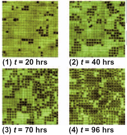 |
| Four images from different points in time during an island growth experiment. |
Abstract:
Watching crystals grow provides clues to making smoother, defect-free thin films
Growing crystals with colloids
Ithaca, NY | Posted on January 22nd, 2010To make thin films for semiconductors in electronic devices, layers of atoms must be grown in neat, crystalline sheets. But while some materials grow smooth crystals, others tend to develop bumps and defects -- a serious problem for thin-film manufacturing.
In the Jan. 22 online edition of the journal Science, Cornell researchers shed new light on how atoms arrange themselves into thin films. Led by assistant professor of physics Itai Cohen, they recreated conditions of layer-by-layer crystalline growth using particles much bigger than atoms, but still small enough that they behave like atoms.
"These particles are big and slow enough that you can see what's going on in real time," explained graduate student Mark Buckley.
Using an optical microscope, the scientists could watch exactly what their "atoms" -- actually, micron-sized silica particles suspended in fluid -- did as they crystallized. What's more, they were able to manipulate particles one at a time and test conditions that led to smooth crystal growth. In doing so, they discovered that the random darting motion of the particles is a key factor that affects how the crystals grow.
A major challenge to growing thin films with atoms is that the atoms often form mounds, rather than crystallizing into thin sheets. This happens because as atoms are deposited onto a substrate, they initially form small crystals, called islands. When more atoms are dumped on top of these crystals, the atoms tend to stay atop the islands, rather than hopping off the edges -- as though there were a barrier on the crystals' edges. This creates the pesky rough spots, "and it's game over" for a perfect thin film, Cohen said.
Conventional theory says atoms that land on top of islands feel an energetic "pull" from other atoms that keeps them from rolling off. In their colloidal system, the researchers eliminated this pull by shortening the bonds between their particles. But they still saw their particles hesitate at the islands' edges.
Further analysis using optical tweezers to manipulate individual particles allowed the researchers to measure just how long it took for particles to move off the crystal islands. Because the particles were suspended in a fluid, they were knocked about in what's called Brownian motion, which is like a random walk.
As the particles moved and diffused from one area to another, the researchers noted that the distance a particle had to travel to "fall" off an island's edge was three times farther than moving laterally from one site on the island to another.
And because the particles had to go this distance in a Brownian fashion, it took them nine times longer to complete this "fall." This difference in time explained why the researchers still saw a barrier at their island edges.
Atoms on a crystalline film move in a manner similar to Brownian particles, since the vibrations of the underlying crystal, called phonons, tend to jostle them about. The researchers surmised that in addition to the bonding between the atoms, this random motion may also contribute to the barrier at the crystals' edges, and hence the roughness in the crystal film.
"If the principles we have uncovered can be applied to the atomic scale, scientists will be able to better control the growth of thin films used to manufacture electronic components for our computers and cell phones," Cohen said.
The paper's co-authors are former postdoctoral associate Rajesh Ganapathy, now a faculty member at the Jawaharlal Nehru Centre for Advanced Scientific Research in Bangalore, India, and graduate students Sharon Gerbode and Mark Buckley. The work was funded by King Abdullah University of Science and Technology, the Cornell Center for Materials Research, National Science Foundation and the Cornell NanoScale Science and Technology Facility.
####
About Cornell University
Once called "the first American university" by educational historian Frederick Rudolph, Cornell University represents a distinctive mix of eminent scholarship and democratic ideals. Adding practical subjects to the classics and admitting qualified students regardless of nationality, race, social circumstance, gender, or religion was quite a departure when Cornell was founded in 1865.
Today's Cornell reflects this heritage of egalitarian excellence. It is home to the nation's first colleges devoted to hotel administration, industrial and labor relations, and veterinary medicine. Both a private university and the land-grant institution of New York State, Cornell University is the most educationally diverse member of the Ivy League.
On the Ithaca campus alone nearly 20,000 students representing every state and 120 countries choose from among 4,000 courses in 11 undergraduate, graduate, and professional schools. Many undergraduates participate in a wide range of interdisciplinary programs, play meaningful roles in original research, and study in Cornell programs in Washington, New York City, and the world over.
For more information, please click here
Contacts:
Media Contact:
Blaine Friedlander
(607) 254-8093
Cornell Chronicle:
Anne Ju
(607) 255-9735
Copyright © Cornell University
If you have a comment, please Contact us.Issuers of news releases, not 7th Wave, Inc. or Nanotechnology Now, are solely responsible for the accuracy of the content.
Bookmark:


| Related News Press |
News and information
![]() Simulating magnetization in a Heisenberg quantum spin chain April 5th, 2024
Simulating magnetization in a Heisenberg quantum spin chain April 5th, 2024
![]() NRL charters Navy�s quantum inertial navigation path to reduce drift April 5th, 2024
NRL charters Navy�s quantum inertial navigation path to reduce drift April 5th, 2024
![]() Discovery points path to flash-like memory for storing qubits: Rice find could hasten development of nonvolatile quantum memory April 5th, 2024
Discovery points path to flash-like memory for storing qubits: Rice find could hasten development of nonvolatile quantum memory April 5th, 2024
![]() Good as gold - improving infectious disease testing with gold nanoparticles April 5th, 2024
Good as gold - improving infectious disease testing with gold nanoparticles April 5th, 2024
Thin films
![]() Utilizing palladium for addressing contact issues of buried oxide thin film transistors April 5th, 2024
Utilizing palladium for addressing contact issues of buried oxide thin film transistors April 5th, 2024
![]() Understanding the mechanism of non-uniform formation of diamond film on tools: Paving the way to a dry process with less environmental impact March 24th, 2023
Understanding the mechanism of non-uniform formation of diamond film on tools: Paving the way to a dry process with less environmental impact March 24th, 2023
![]() New study introduces the best graphite films: The work by Distinguished Professor Feng Ding at UNIST has been published in the October 2022 issue of Nature Nanotechnology November 4th, 2022
New study introduces the best graphite films: The work by Distinguished Professor Feng Ding at UNIST has been published in the October 2022 issue of Nature Nanotechnology November 4th, 2022
Govt.-Legislation/Regulation/Funding/Policy
![]() NRL charters Navy�s quantum inertial navigation path to reduce drift April 5th, 2024
NRL charters Navy�s quantum inertial navigation path to reduce drift April 5th, 2024
![]() Discovery points path to flash-like memory for storing qubits: Rice find could hasten development of nonvolatile quantum memory April 5th, 2024
Discovery points path to flash-like memory for storing qubits: Rice find could hasten development of nonvolatile quantum memory April 5th, 2024
![]() Chemical reactions can scramble quantum information as well as black holes April 5th, 2024
Chemical reactions can scramble quantum information as well as black holes April 5th, 2024
Chip Technology
![]() Discovery points path to flash-like memory for storing qubits: Rice find could hasten development of nonvolatile quantum memory April 5th, 2024
Discovery points path to flash-like memory for storing qubits: Rice find could hasten development of nonvolatile quantum memory April 5th, 2024
![]() Utilizing palladium for addressing contact issues of buried oxide thin film transistors April 5th, 2024
Utilizing palladium for addressing contact issues of buried oxide thin film transistors April 5th, 2024
![]() HKUST researchers develop new integration technique for efficient coupling of III-V and silicon February 16th, 2024
HKUST researchers develop new integration technique for efficient coupling of III-V and silicon February 16th, 2024
Nanoelectronics
![]() Interdisciplinary: Rice team tackles the future of semiconductors Multiferroics could be the key to ultralow-energy computing October 6th, 2023
Interdisciplinary: Rice team tackles the future of semiconductors Multiferroics could be the key to ultralow-energy computing October 6th, 2023
![]() Key element for a scalable quantum computer: Physicists from Forschungszentrum J�lich and RWTH Aachen University demonstrate electron transport on a quantum chip September 23rd, 2022
Key element for a scalable quantum computer: Physicists from Forschungszentrum J�lich and RWTH Aachen University demonstrate electron transport on a quantum chip September 23rd, 2022
![]() Reduced power consumption in semiconductor devices September 23rd, 2022
Reduced power consumption in semiconductor devices September 23rd, 2022
![]() Atomic level deposition to extend Moore�s law and beyond July 15th, 2022
Atomic level deposition to extend Moore�s law and beyond July 15th, 2022
Announcements
![]() NRL charters Navy�s quantum inertial navigation path to reduce drift April 5th, 2024
NRL charters Navy�s quantum inertial navigation path to reduce drift April 5th, 2024
![]() Discovery points path to flash-like memory for storing qubits: Rice find could hasten development of nonvolatile quantum memory April 5th, 2024
Discovery points path to flash-like memory for storing qubits: Rice find could hasten development of nonvolatile quantum memory April 5th, 2024
|
|
||
|
|
||
| The latest news from around the world, FREE | ||
|
|
||
|
|
||
| Premium Products | ||
|
|
||
|
Only the news you want to read!
Learn More |
||
|
|
||
|
Full-service, expert consulting
Learn More |
||
|
|
||