Home > Press > Nanoscience goes 'big'
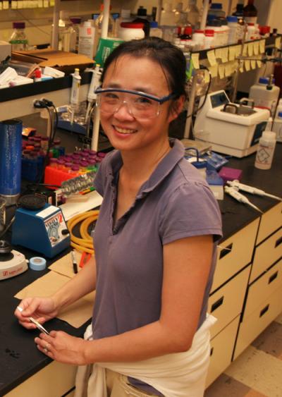 |
| Jen Cha, a UC San Diego nanoengineering professor, is pushing the envelop in nanoscience by using biology to engineer the assembly of nanoscale materials for applications in medicine, electronics and energy. Credit: UC San Diego |
Abstract:
UCSD nanoengineering discovery could lead to enhanced electronics
Nanoscience goes 'big'
San Diego, CA | Posted on January 8th, 2010Nanoscience has the potential to play an enormous role in enhancing a range of products, including sensors, photovoltaics and consumer electronics. Scientists in this field have created a multitude of nano scale materials, such as metal nanocrystals, carbon nanotubes and semiconducting nanowires. However, despite their appeal, it has remained an astounding challenge to engineer the orientation and placement of these materials into the desired device architectures that are reproducible in high yields and at low costs - until now. Jen Cha, a UC San Diego nanoengineering professor, and her team of researchers, have discovered that one way to bridge this gap is to use biomolecules, such as DNA and proteins. Details of this discovery were recently published in a paper titled "Large Area Spatially Ordered Arrays of Gold Nanoparticles Directed by Lithographically Confined DNA Origami," in Nature Nanotechology.
"Self-assembled structures are often too small and affordable lithographic patterns are too large," said Albert Hung, lead author of the Nature Nanotechnology paper and a post doc working in Cha's lab. "But rationally designed synthetic DNA nanostructures allow us to access length scales between 5 and 100 nanometers and bridge the two systems.
"People have created a huge variety of unique and functional nanostructures, but for some intended applications they are worthless unless you can place individual structures, billions or trillions of them at the same time, at precise locations," Hung added. "We hope that our research brings us a step closer to solving this very difficult problem."
Hung said the recently discovered method may be useful for fabricating nanoscale electronic or optical circuits and multiplex sensors.
"A number of groups have worked on parts of this research problem before, but to our knowledge, we're the first to attempt to address so many parts together as a whole," he said.
One of the main applications of this research that Cha and her group are interested in is for sensing. "There is no foreseeable route to be able to build a complex array of different nanoscale sensing elements currently," said Cha, a former IBM research scientist who joined the UCSD Jacobs School of Engineering faculty in 2008. "Our work is one of the first clear examples of how you can merge top down lithography with bottom up self assembly to build such an array. That means that you have a substrate that is patterned by conventional lithography, and then you need to take that pattern and merge it with something that can direct the assembly of even smaller objects, such as those having dimensions between 2 and 20 nanometers. You need an intermediate template, which is the DNA origami, which has the ability to bind to something else much smaller and direct their assembly into the desired configuration. This means we can potentially build transistors from carbon nanotubes and also possibly use nanostructures to detect certain proteins in solutions. Scientists have been talking about patterning different sets of proteins on a substrate and now we have the ability to do that."
Cha said the next step would be to actually develop a device based on this research method.
"I'm very interested in the applications of this research and we're working our way to get there," she said.
For the last 6 years, Cha's research has focused on using biology to engineer the assembly of nanoscale materials for applications in medicine, electronics and energy. One of the limitations of nanoscience is it doesn't allow mass production of products, but Cha's work is focused on trying figure out how to do that and do it cheaply. Much of her recent work has focused on using DNA to build 2D structures.
"Using DNA to assemble materials is an area that many people are excited about," Cha said. "You can fold DNA into anything you want - for example, you can build a large scaffold and within that you could assemble very small objects such as nano particles, nano wires or proteins.
"Engineers need to understand the physical forces needed to build functional arrays from functional materials," she added. "My job as a nanoengineer is to figure out what you need to do to put all the different parts together, whether it's a drug delivery vehicle, photovoltaic applications, sensors or transistors. We need to think about ways to take all the nano materials and engineer them it into something people can use and hold."
Large-area spatially ordered arrays of gold nanoparticles directed by lithographically confined DNA origami, Nature Nanotechnology, Albert M. Hung, Christine M. Micheel, Luisa D. Bozano, Lucas W. Osterbur, Greg M. Wallraff2 & Jennifer N. Cha
####
For more information, please click here
Copyright © Eurekalert
If you have a comment, please Contact us.Issuers of news releases, not 7th Wave, Inc. or Nanotechnology Now, are solely responsible for the accuracy of the content.
Bookmark:


| Related News Press |
News and information
![]() Simulating magnetization in a Heisenberg quantum spin chain April 5th, 2024
Simulating magnetization in a Heisenberg quantum spin chain April 5th, 2024
![]() NRL charters Navy�s quantum inertial navigation path to reduce drift April 5th, 2024
NRL charters Navy�s quantum inertial navigation path to reduce drift April 5th, 2024
![]() Discovery points path to flash-like memory for storing qubits: Rice find could hasten development of nonvolatile quantum memory April 5th, 2024
Discovery points path to flash-like memory for storing qubits: Rice find could hasten development of nonvolatile quantum memory April 5th, 2024
Possible Futures
![]() Discovery points path to flash-like memory for storing qubits: Rice find could hasten development of nonvolatile quantum memory April 5th, 2024
Discovery points path to flash-like memory for storing qubits: Rice find could hasten development of nonvolatile quantum memory April 5th, 2024
![]() With VECSELs towards the quantum internet Fraunhofer: IAF achieves record output power with VECSEL for quantum frequency converters April 5th, 2024
With VECSELs towards the quantum internet Fraunhofer: IAF achieves record output power with VECSEL for quantum frequency converters April 5th, 2024
Chip Technology
![]() Discovery points path to flash-like memory for storing qubits: Rice find could hasten development of nonvolatile quantum memory April 5th, 2024
Discovery points path to flash-like memory for storing qubits: Rice find could hasten development of nonvolatile quantum memory April 5th, 2024
![]() Utilizing palladium for addressing contact issues of buried oxide thin film transistors April 5th, 2024
Utilizing palladium for addressing contact issues of buried oxide thin film transistors April 5th, 2024
![]() HKUST researchers develop new integration technique for efficient coupling of III-V and silicon February 16th, 2024
HKUST researchers develop new integration technique for efficient coupling of III-V and silicon February 16th, 2024
Self Assembly
![]() Liquid crystal templated chiral nanomaterials October 14th, 2022
Liquid crystal templated chiral nanomaterials October 14th, 2022
![]() Nanoclusters self-organize into centimeter-scale hierarchical assemblies April 22nd, 2022
Nanoclusters self-organize into centimeter-scale hierarchical assemblies April 22nd, 2022
![]() Atom by atom: building precise smaller nanoparticles with templates March 4th, 2022
Atom by atom: building precise smaller nanoparticles with templates March 4th, 2022
![]() Nanostructures get complex with electron equivalents: Nanoparticles of two different sizes break away from symmetrical designs January 14th, 2022
Nanostructures get complex with electron equivalents: Nanoparticles of two different sizes break away from symmetrical designs January 14th, 2022
Nanotubes/Buckyballs/Fullerenes/Nanorods/Nanostrings
![]() Tests find no free-standing nanotubes released from tire tread wear September 8th, 2023
Tests find no free-standing nanotubes released from tire tread wear September 8th, 2023
![]() Detection of bacteria and viruses with fluorescent nanotubes July 21st, 2023
Detection of bacteria and viruses with fluorescent nanotubes July 21st, 2023
Sensors
Nanoelectronics
![]() Interdisciplinary: Rice team tackles the future of semiconductors Multiferroics could be the key to ultralow-energy computing October 6th, 2023
Interdisciplinary: Rice team tackles the future of semiconductors Multiferroics could be the key to ultralow-energy computing October 6th, 2023
![]() Key element for a scalable quantum computer: Physicists from Forschungszentrum J�lich and RWTH Aachen University demonstrate electron transport on a quantum chip September 23rd, 2022
Key element for a scalable quantum computer: Physicists from Forschungszentrum J�lich and RWTH Aachen University demonstrate electron transport on a quantum chip September 23rd, 2022
![]() Reduced power consumption in semiconductor devices September 23rd, 2022
Reduced power consumption in semiconductor devices September 23rd, 2022
![]() Atomic level deposition to extend Moore�s law and beyond July 15th, 2022
Atomic level deposition to extend Moore�s law and beyond July 15th, 2022
Discoveries
![]() Chemical reactions can scramble quantum information as well as black holes April 5th, 2024
Chemical reactions can scramble quantum information as well as black holes April 5th, 2024
![]() New micromaterial releases nanoparticles that selectively destroy cancer cells April 5th, 2024
New micromaterial releases nanoparticles that selectively destroy cancer cells April 5th, 2024
![]() Utilizing palladium for addressing contact issues of buried oxide thin film transistors April 5th, 2024
Utilizing palladium for addressing contact issues of buried oxide thin film transistors April 5th, 2024
Announcements
![]() NRL charters Navy�s quantum inertial navigation path to reduce drift April 5th, 2024
NRL charters Navy�s quantum inertial navigation path to reduce drift April 5th, 2024
![]() Discovery points path to flash-like memory for storing qubits: Rice find could hasten development of nonvolatile quantum memory April 5th, 2024
Discovery points path to flash-like memory for storing qubits: Rice find could hasten development of nonvolatile quantum memory April 5th, 2024
|
|
||
|
|
||
| The latest news from around the world, FREE | ||
|
|
||
|
|
||
| Premium Products | ||
|
|
||
|
Only the news you want to read!
Learn More |
||
|
|
||
|
Full-service, expert consulting
Learn More |
||
|
|
||