Home > Press > IMEC unveils promising mechanically-stacked GaAs/Ge multijunction solar cell
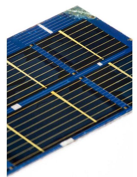 |
| IMEC's mechanically stacked GaAs/Ge cell |
Abstract:
At the European Photovoltaic Solar Energy Conference (Hamburg, Germany), IMEC presents a mechanically-stacked GaAs/Ge multijunction solar cell. This is the first promising demonstrator of IMEC's novel technology to produce mechanically stacked, high-efficiency multijunction solar cells, aiming at efficiencies above 40%.
IMEC unveils promising mechanically-stacked GaAs/Ge multijunction solar cell
Leuven, Belgium | Posted on September 22nd, 2009At the top of the stack is a one-side contacted GaAs top cell that is only 4�m thick and that is transparent for infrared light. Its efficiency is 23.4%, which is close to the efficiency of standard GaAs cells. IMEC has succeeded in transferring this GaAs top cell onto a Ge bottom cell, creating a mechanical stack. In that stack, the Ge bottom cell is separately contacted. It has a potential efficiency of 3-3.5%, which is higher than Ge bottom cells in state-of-the-art monolithically stacked InGaP/(In)GaAs/Ge cells. Looking forward, Giovanni Flamand, team manager at IMEC, expects to show a first working triple-junction cell beginning of 2010.
This cell is a demonstrator of IMEC's innovative technology to produce mechanically stacked, high-efficiency InGaP/GaAs/Ge triple-junction solar cells. This includes manufacturing world-class thin-film III-V cells and Ge bottom cells, and developing a technology to mechanically stack them. The expected conversion efficiencies are 1-2% higher than those obtained today with monolithic triple-junction solar cells (> 40% with concentrated illumination). In addition, the new cells show an enhanced spectral robustness. Stacked solar cells combine cells made from different materials to capture and converse a larger part of the light spectrum than is possible with a single material.
Dr. Jef Poortmans, IMEC's Photovoltaics Program Director: "Mechanical stacks are more complex to handle and interconnect. But they definitely offer a way to increase the conversion efficiency and energy yield of high-efficiency solar cells. And they also enable an efficient way to try and use new combinations of materials. For this technology, we profit from IMEC's expertise in 3D stacking, growing III-V layers, and solar cell processing."
####
About IMEC
IMEC is a world-leading independent research center in nanoelectronics and nanotechnology. IMEC is headquartered in Leuven, Belgium, and has offices in Belgium, the Netherlands, Taiwan, US, China and Japan. Its staff of more than 1,650 people include over 550 industrial residents and guest researchers. In 2008, IMEC's revenue (P&L) was 270 million euro.
IMEC's More Moore research targets semiconductor scaling for the 22nm technology node and beyond. With its More than Moore research, IMEC invents technology for nomadic embedded systems, wireless autonomous transducer solutions, biomedical electronics, photovoltaics, organic electronics and GaN power electronics.
IMEC's research bridges the gap between the fundamental research at universities and R&D in the industry. It has unique processing and system know-how, intellectual property portfolio, state-of-the-art infrastructure, and a strong and worldwide network position. This makes IMEC a key partner for shaping the technology of the future.
IMEC is a registered trademark for the activities of IMEC International (a legal entity set up under Belgian law as a "stichting van openbaar nut"), IMEC in Belgium (IMEC vzw supported by the Flemish Government), stichting IMEC Nederland (IMEC-NL) and IMEC Taiwan Co. (IMEC-TW).
For more information, please click here
Contacts:
IMEC : Katrien Marent, Director of External Communications, T: +32 16 28 18 80, Mobile : +32 474 30 28 66,
Copyright © IMEC
If you have a comment, please Contact us.Issuers of news releases, not 7th Wave, Inc. or Nanotechnology Now, are solely responsible for the accuracy of the content.
Bookmark:


| Related News Press |
News and information
![]() Simulating magnetization in a Heisenberg quantum spin chain April 5th, 2024
Simulating magnetization in a Heisenberg quantum spin chain April 5th, 2024
![]() NRL charters Navy�s quantum inertial navigation path to reduce drift April 5th, 2024
NRL charters Navy�s quantum inertial navigation path to reduce drift April 5th, 2024
![]() Discovery points path to flash-like memory for storing qubits: Rice find could hasten development of nonvolatile quantum memory April 5th, 2024
Discovery points path to flash-like memory for storing qubits: Rice find could hasten development of nonvolatile quantum memory April 5th, 2024
Possible Futures
![]() Discovery points path to flash-like memory for storing qubits: Rice find could hasten development of nonvolatile quantum memory April 5th, 2024
Discovery points path to flash-like memory for storing qubits: Rice find could hasten development of nonvolatile quantum memory April 5th, 2024
![]() With VECSELs towards the quantum internet Fraunhofer: IAF achieves record output power with VECSEL for quantum frequency converters April 5th, 2024
With VECSELs towards the quantum internet Fraunhofer: IAF achieves record output power with VECSEL for quantum frequency converters April 5th, 2024
Announcements
![]() NRL charters Navy�s quantum inertial navigation path to reduce drift April 5th, 2024
NRL charters Navy�s quantum inertial navigation path to reduce drift April 5th, 2024
![]() Discovery points path to flash-like memory for storing qubits: Rice find could hasten development of nonvolatile quantum memory April 5th, 2024
Discovery points path to flash-like memory for storing qubits: Rice find could hasten development of nonvolatile quantum memory April 5th, 2024
Energy
![]() Development of zinc oxide nanopagoda array photoelectrode: photoelectrochemical water-splitting hydrogen production January 12th, 2024
Development of zinc oxide nanopagoda array photoelectrode: photoelectrochemical water-splitting hydrogen production January 12th, 2024
![]() Shedding light on unique conduction mechanisms in a new type of perovskite oxide November 17th, 2023
Shedding light on unique conduction mechanisms in a new type of perovskite oxide November 17th, 2023
![]() Inverted perovskite solar cell breaks 25% efficiency record: Researchers improve cell efficiency using a combination of molecules to address different November 17th, 2023
Inverted perovskite solar cell breaks 25% efficiency record: Researchers improve cell efficiency using a combination of molecules to address different November 17th, 2023
![]() The efficient perovskite cells with a structured anti-reflective layer � another step towards commercialization on a wider scale October 6th, 2023
The efficient perovskite cells with a structured anti-reflective layer � another step towards commercialization on a wider scale October 6th, 2023
Events/Classes
![]() Researchers demonstrate co-propagation of quantum and classical signals: Study shows that quantum encryption can be implemented in existing fiber networks January 20th, 2023
Researchers demonstrate co-propagation of quantum and classical signals: Study shows that quantum encryption can be implemented in existing fiber networks January 20th, 2023
Solar/Photovoltaic
![]() Development of zinc oxide nanopagoda array photoelectrode: photoelectrochemical water-splitting hydrogen production January 12th, 2024
Development of zinc oxide nanopagoda array photoelectrode: photoelectrochemical water-splitting hydrogen production January 12th, 2024
![]() Shedding light on unique conduction mechanisms in a new type of perovskite oxide November 17th, 2023
Shedding light on unique conduction mechanisms in a new type of perovskite oxide November 17th, 2023
![]() Inverted perovskite solar cell breaks 25% efficiency record: Researchers improve cell efficiency using a combination of molecules to address different November 17th, 2023
Inverted perovskite solar cell breaks 25% efficiency record: Researchers improve cell efficiency using a combination of molecules to address different November 17th, 2023
![]() Charged �molecular beasts� the basis for new compounds: Researchers at Leipzig University use �aggressive� fragments of molecular ions for chemical synthesis November 3rd, 2023
Charged �molecular beasts� the basis for new compounds: Researchers at Leipzig University use �aggressive� fragments of molecular ions for chemical synthesis November 3rd, 2023
|
|
||
|
|
||
| The latest news from around the world, FREE | ||
|
|
||
|
|
||
| Premium Products | ||
|
|
||
|
Only the news you want to read!
Learn More |
||
|
|
||
|
Full-service, expert consulting
Learn More |
||
|
|
||