Home > Press > Fast transistors for the digital world
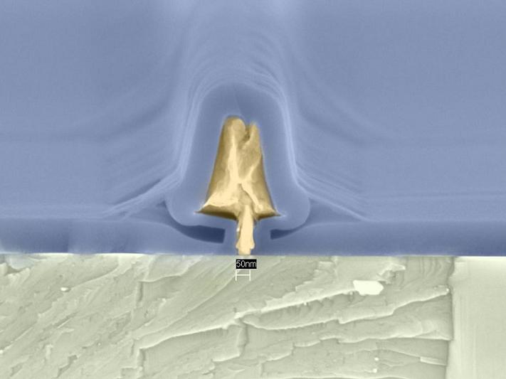 |
| Photo of a transistor cross-section. Such cross-sections are used to characterize the fabrication process. The transistor is wrapped in a passivation film out of silicon nitride (SiN) intended to protect it from the elements (Photo: ETH Zurich). |
Abstract:
Our society is insatiable as far as the transfer of data is concerned. Consequently, increasingly faster and cheaper transistors are being developed. In row in recent months, researchers from ETH Zurich have now broken the world record for the switching speed of nitride-based transistors that use silicon as a substrate several times.
Fast transistors for the digital world
Zurich | Posted on September 14th, 2009Although Youtube was for example only founded in 2005, 100 million videos are watched daily on its platform, and the amount of digital information in our society is constantly rising. In 2006, for example, 161 billion gigabytes of digital information were produced - three million times as much information ever stored in books. What's more, by 2010 this figure will already have increased to about 1000 billion gigabytes per year.
Few people are aware that not only does one always need better software to process such enormous amounts of data, but that the demands on hardware also continually increase. Transistors are pivotal elements in this struggle: small semiconductor components that can be controlled through the flow of electrons to work like microscopic switches or amplifiers in the nanometer scale.
Faster and faster the goal
Colombo Bolognesi, Professor of TeraHertz Electronics at the Laboratory of Electromagnetic Fields and Microwave Electronics, and his group are experts when it comes to fast transistors. Their goal is to improve their speed of operation. After all, the faster a transistor operates, the more information it can process in a given time. The researchers therefore combine semiconductor materials in different layers to enable the electrons to flow as quickly as possible. They also try to make the transistors as small as possible so that the electrons travel shorter distances, thereby enhancing the operation speed of the devices. These semiconductor layers have to be prepared under the cleanest conditions as they are often only as thick as a few atomic layers. Bolognesi's research group is thus one of the principal users of the FIRST Lab (www.first.ethz.ch/) on the H�nggerberg. One of the special transistor technologies that Bolognesi's group is working on is based on aluminium gallium nitride (AlGaN/GaN) and has high electron mobility, thus belonging to the "High Electron Mobility Transistors (HEMTs)" class of transistors.
AlGaN/GaN HEMTs are of technological importance because they can support large current flows and high voltages while remaining functional at elevated temperatures. Over the last few months, Bolognesi and his students have managed to beat the record for the switching speed of AlGaN/GaN HEMTs on silicon substrates several times in a row: the record is now 108 GHz. "Other groups had only managed 28 GHz up to now using similar technology, so we are almost four times as fast", says Bolognesi, putting his team's achievement into perspective.
Price is the deciding factor
Usually, sapphire or silicon carbide is used as the substrate material for AlGaN/GaN HEMTs. However, in consumer electronics the part price plays a big role, as does device performance. For large scale production, every cent you save on a transistor means a better profit. This is why intensive research is being conducted worldwide on realizing efficient AlGaN/GaN transistors on low-cost silicon substrates.
Silicon is cheaper than the customary substrates currently available as it is extremely abundant in nature, constituting about 26 percent by weight of the earth's crust. For Bolognesi, likely high-volume applications for AlGaN/GaN HEMTs on silicon will be in automotive anti-collision radars which operate at 77 GHz, or in mobile telephone base station transmitter systems. In particular, such transmitters could save energy through components that also work with a much better efficiency than currently available alternatives. This would not only be good for the mobile phone operators' wallets, but also for the environment. However, Bolognesi states that the direct commercial application is not the primary aim of his team's research: "We are looking to demonstrate what is possible in practically manufacturable devices while trying to push their physical limits of operation."
Transistors for space applications and optical networks
Bolognesi and his team do not only seek to break transistor performance records; they also develop transistors for practical applications -Indium Phosphide HEMTs, for instance, which are used in astronomical applications. Bolognesi's team produces special low-noise transistors for the Deep Space Network on behalf of the European Space Agency (ESA). American aerospace companies are actually the leaders in the field but, as their transistor technology is also applied in intelligence satellites, it cannot be sold abroad. The ESA therefore relies on ETH Zurich's expertise for some of its systems.
Bolognesi and his group are also active in the field of bipolar transistors, which are used in optic networks. Currently, the highest transmission rate for optic networks is 100-150 Gb/s in the lab (10-40 Gb/s in commercial systems). If Bolognesi's team succeeds in improving the speed of bipolar transistors to 1 Terahertz, however, the transmission rate would double to reach 300 Gb/s or more.
####
About ETH Zurich
ETH Zurich (German: Eidgen�ssische Technische Hochschule Z�rich) or Swiss Federal Institute of Technology Zurich is a science and technology university in the City of Zurich, Switzerland. Locals sometimes refer to it by the name Poly, derived from the original name Eidgen�ssisches Polytechnikum or Federal Polytechnic Institute.
From Wikipedia, the free encyclopedia
For more information, please click here
Contacts:
ETH Zurich
Editorial Office
HG F 41
Raemistrasse 101
8092 Zurich
SWITZERLAND
Fax +41 44 632 17 16
Copyright © ETH Zurich
If you have a comment, please Contact us.Issuers of news releases, not 7th Wave, Inc. or Nanotechnology Now, are solely responsible for the accuracy of the content.
Bookmark:


| Related Links |
| Related News Press |
News and information
![]() Simulating magnetization in a Heisenberg quantum spin chain April 5th, 2024
Simulating magnetization in a Heisenberg quantum spin chain April 5th, 2024
![]() NRL charters Navy�s quantum inertial navigation path to reduce drift April 5th, 2024
NRL charters Navy�s quantum inertial navigation path to reduce drift April 5th, 2024
![]() Discovery points path to flash-like memory for storing qubits: Rice find could hasten development of nonvolatile quantum memory April 5th, 2024
Discovery points path to flash-like memory for storing qubits: Rice find could hasten development of nonvolatile quantum memory April 5th, 2024
Possible Futures
![]() Discovery points path to flash-like memory for storing qubits: Rice find could hasten development of nonvolatile quantum memory April 5th, 2024
Discovery points path to flash-like memory for storing qubits: Rice find could hasten development of nonvolatile quantum memory April 5th, 2024
![]() With VECSELs towards the quantum internet Fraunhofer: IAF achieves record output power with VECSEL for quantum frequency converters April 5th, 2024
With VECSELs towards the quantum internet Fraunhofer: IAF achieves record output power with VECSEL for quantum frequency converters April 5th, 2024
Chip Technology
![]() Discovery points path to flash-like memory for storing qubits: Rice find could hasten development of nonvolatile quantum memory April 5th, 2024
Discovery points path to flash-like memory for storing qubits: Rice find could hasten development of nonvolatile quantum memory April 5th, 2024
![]() Utilizing palladium for addressing contact issues of buried oxide thin film transistors April 5th, 2024
Utilizing palladium for addressing contact issues of buried oxide thin film transistors April 5th, 2024
![]() HKUST researchers develop new integration technique for efficient coupling of III-V and silicon February 16th, 2024
HKUST researchers develop new integration technique for efficient coupling of III-V and silicon February 16th, 2024
Nanoelectronics
![]() Interdisciplinary: Rice team tackles the future of semiconductors Multiferroics could be the key to ultralow-energy computing October 6th, 2023
Interdisciplinary: Rice team tackles the future of semiconductors Multiferroics could be the key to ultralow-energy computing October 6th, 2023
![]() Key element for a scalable quantum computer: Physicists from Forschungszentrum J�lich and RWTH Aachen University demonstrate electron transport on a quantum chip September 23rd, 2022
Key element for a scalable quantum computer: Physicists from Forschungszentrum J�lich and RWTH Aachen University demonstrate electron transport on a quantum chip September 23rd, 2022
![]() Reduced power consumption in semiconductor devices September 23rd, 2022
Reduced power consumption in semiconductor devices September 23rd, 2022
![]() Atomic level deposition to extend Moore�s law and beyond July 15th, 2022
Atomic level deposition to extend Moore�s law and beyond July 15th, 2022
Announcements
![]() NRL charters Navy�s quantum inertial navigation path to reduce drift April 5th, 2024
NRL charters Navy�s quantum inertial navigation path to reduce drift April 5th, 2024
![]() Discovery points path to flash-like memory for storing qubits: Rice find could hasten development of nonvolatile quantum memory April 5th, 2024
Discovery points path to flash-like memory for storing qubits: Rice find could hasten development of nonvolatile quantum memory April 5th, 2024
Aerospace/Space
![]() Under pressure - space exploration in our time: Advancing space exploration through diverse collaborations and ethical policies February 16th, 2024
Under pressure - space exploration in our time: Advancing space exploration through diverse collaborations and ethical policies February 16th, 2024
![]() Bridging light and electrons January 12th, 2024
Bridging light and electrons January 12th, 2024
![]() Manufacturing advances bring material back in vogue January 20th, 2023
Manufacturing advances bring material back in vogue January 20th, 2023
Photonics/Optics/Lasers
![]() With VECSELs towards the quantum internet Fraunhofer: IAF achieves record output power with VECSEL for quantum frequency converters April 5th, 2024
With VECSELs towards the quantum internet Fraunhofer: IAF achieves record output power with VECSEL for quantum frequency converters April 5th, 2024
![]() Nanoscale CL thermometry with lanthanide-doped heavy-metal oxide in TEM March 8th, 2024
Nanoscale CL thermometry with lanthanide-doped heavy-metal oxide in TEM March 8th, 2024
![]() Optically trapped quantum droplets of light can bind together to form macroscopic complexes March 8th, 2024
Optically trapped quantum droplets of light can bind together to form macroscopic complexes March 8th, 2024
![]() HKUST researchers develop new integration technique for efficient coupling of III-V and silicon February 16th, 2024
HKUST researchers develop new integration technique for efficient coupling of III-V and silicon February 16th, 2024
|
|
||
|
|
||
| The latest news from around the world, FREE | ||
|
|
||
|
|
||
| Premium Products | ||
|
|
||
|
Only the news you want to read!
Learn More |
||
|
|
||
|
Full-service, expert consulting
Learn More |
||
|
|
||