Home > Press > Material world: graphene’s versatility promises new applications
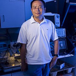 |
| N.J. Tao, director of the Center for Bioelectronics and Biosensors, has experimentally measured an important property of graphene. |
Abstract:
Since its discovery just a few years ago, graphene has climbed to the top of the heap of new super-materials poised to transform the electronics and nanotechnology landscape.
Material world: graphene’s versatility promises new applications
Tempe, AZ | Posted on August 6th, 2009As N.J. Tao, a researcher at the Biodesign Institute of Arizona State University explains, this two-dimensional honeycomb structure of carbon atoms is exceptionally strong and versatile. Its unusual properties make it ideal for applications that are pushing the existing limits of microchips, chemical sensing instruments, biosensors, ultracapacitance devices, flexible displays and other innovations.
In the latest issue of Nature Nanotechnology Letters, Tao describes the first direct measurement of a fundamental property of graphene, known as quantum capacitance, using an electrochemical gate method. A better understanding of this crucial variable should prove invaluable to other investigators participating in what amounts to a gold rush of graphene research.
Although theoretical work on single atomic layer graphene-like structures has been going on for decades, the discovery of real graphene came as a shock. "When they found it was a stable material at room temperature," Tao says, "everyone was surprised." As it happens, minute traces of graphene are shed whenever a pencil line is drawn, though producing a 2-D sheet of the material has proven trickier. Graphene is remarkable in terms of thinness and resiliency. A one-atom thick graphene sheet sufficient in size to cover a football field, would weigh less than a gram. It is also the strongest material in nature—roughly 200 times the strength of steel. Most of the excitement however, has to do with the unusual electronic properties of the material.
Graphene displays outstanding electron transport, permitting electricity to flow rapidly and more or less unimpeded through the material. In fact, electrons have been shown to behave as massless particles similar to photons, zipping across a graphene layer without scattering. This property is critical for many device applications and has prompted speculation that graphene could eventually supplant silicon as the substance of choice for computer chips, offering the prospect of ultrafast computers operating at terahertz speeds, rocketing past current gigahertz chip technology. Yet, despite encouraging progress, a thorough understanding of graphene's electronic properties has remained elusive. Tao stresses that quantum capacitance measurements are an essential part of this understanding.
Capacitance is a material's ability to store energy. In classical physics, capacitance is limited by the repulsion of like electrical charges, for example, electrons. The more charge you put into a device, the more energy you have to expend to contain it, in order to overcome charge repulsion. However, another kind of capacitance exists, and dominates overall capacitance in a two-dimensional material like graphene. This quantum capacitance is the result of the Pauli exclusion principle, which states that two fermions—a class of common particles including protons, neutrons and electrons—cannot occupy the same location at the same time. Once a quantum state is filled, subsequent fermions are forced to occupy successively higher energy states. As Tao explains, "it's just like in a building, where people are forced to go to the second floor once the first level is occupied."
In the current study, two electrodes were attached to graphene, and a voltage applied across the material's two-dimensional surface by means of a third, gate electrode. Plots of voltage vs. capacitance can be seen in the figure above. In Tao's experiments, graphene's ability to store charge according to the laws of quantum capacitance, were subjected to detailed measurement. The results show that graphene's capacitance is very small. Further, the quantum capacitance of graphene did not precisely duplicate theoretical predictions for the behavior of ideal graphene. This is due to the fact that charged impurities occur in experimental samples of graphene, which alter the behavior relative to what is expected according to theory.
Tao stresses the importance of these charged impurities and what they may mean for the development of graphene devices. Such impurities were already known to affect electron mobility in graphene, though their effect on quantum capacitance has only now been revealed. Low capacitance is particularly desirable for chemical sensing devices and biosensors as it produces a lower signal-to-noise ratio, providing for extremely fine-tuned resolution of chemical or biological agents. Improvements to graphene will allow its electrical behavior to more closely approximate theory. This can be accomplished by adding counter ions to balance the charges resulting from impurities, thereby further lowering capacitance.
The sensitivity of graphene's single atomic layer geometry and low capacitance promise a significant boost for biosensor applications. Such applications are a central topic of interest for Tao, who directs the Biodesign Institute's Center for Bioelectronics and Biosensors. As Tao explains, any biological substance that interacts with graphene's single atom surface layer can be detected, causing a huge change in the properties of the electrons.
One possible biosensor application under consideration would involve functionalizing graphene's surface with antibodies, in order to precisely study their interaction with specific antigens. Such graphene-based biosensors could detect individual binding events, given a suitable sample. For other applications, adding impurities to graphene could raise overall interfacial capacitance. Ultracapacitors made of graphene composites would be capable of storing much larger amounts of renewable energy from solar, wind or wave energy than current technologies permit.
Because of graphene's planar geometry, it may be more compatible with conventional electronic devices than other materials, including the much-vaunted carbon nanotubes. "You can imagine an atomic sheet, cut into different shapes to create different device properties," Tao says.
Since the discovery of graphene, the hunt has been on for similar two-dimensional crystal lattices, though so far, graphene remains a precious oddity.
Advanced Online Publication: www.nature.com/nnano/journal/vaop/ncurrent/full/nnano.2009.177.html
####
About The Biodesign Institute, Arizona State University
The hundreds of researchers at ASU’s Biodesign Institute are driven by a passion to solve some of the world’s most urgent problems affecting human health and the health of our planet:
* Improving health care through more personalized diagnostics and treatment
* Providing renewable sources of energy and cleaning our environment
* Outpacing the global threat of infectious disease, including emerging diseases
* Securing a safer world, particularly through technology that detects threats in advance
For more information, please click here
Contacts:
Written by Richard Harth
Science Writer
Biodesign Institute
Copyright © The Biodesign Institute, Arizona State University
If you have a comment, please Contact us.Issuers of news releases, not 7th Wave, Inc. or Nanotechnology Now, are solely responsible for the accuracy of the content.
Bookmark:


| Related News Press |
News and information
![]() Simulating magnetization in a Heisenberg quantum spin chain April 5th, 2024
Simulating magnetization in a Heisenberg quantum spin chain April 5th, 2024
![]() NRL charters Navy’s quantum inertial navigation path to reduce drift April 5th, 2024
NRL charters Navy’s quantum inertial navigation path to reduce drift April 5th, 2024
![]() Discovery points path to flash-like memory for storing qubits: Rice find could hasten development of nonvolatile quantum memory April 5th, 2024
Discovery points path to flash-like memory for storing qubits: Rice find could hasten development of nonvolatile quantum memory April 5th, 2024
![]() Good as gold - improving infectious disease testing with gold nanoparticles April 5th, 2024
Good as gold - improving infectious disease testing with gold nanoparticles April 5th, 2024
Display technology/LEDs/SS Lighting/OLEDs
![]() Utilizing palladium for addressing contact issues of buried oxide thin film transistors April 5th, 2024
Utilizing palladium for addressing contact issues of buried oxide thin film transistors April 5th, 2024
![]() Light guide plate based on perovskite nanocomposites November 3rd, 2023
Light guide plate based on perovskite nanocomposites November 3rd, 2023
![]() Simple ballpoint pen can write custom LEDs August 11th, 2023
Simple ballpoint pen can write custom LEDs August 11th, 2023
Possible Futures
![]() Discovery points path to flash-like memory for storing qubits: Rice find could hasten development of nonvolatile quantum memory April 5th, 2024
Discovery points path to flash-like memory for storing qubits: Rice find could hasten development of nonvolatile quantum memory April 5th, 2024
![]() With VECSELs towards the quantum internet Fraunhofer: IAF achieves record output power with VECSEL for quantum frequency converters April 5th, 2024
With VECSELs towards the quantum internet Fraunhofer: IAF achieves record output power with VECSEL for quantum frequency converters April 5th, 2024
Chip Technology
![]() Discovery points path to flash-like memory for storing qubits: Rice find could hasten development of nonvolatile quantum memory April 5th, 2024
Discovery points path to flash-like memory for storing qubits: Rice find could hasten development of nonvolatile quantum memory April 5th, 2024
![]() Utilizing palladium for addressing contact issues of buried oxide thin film transistors April 5th, 2024
Utilizing palladium for addressing contact issues of buried oxide thin film transistors April 5th, 2024
![]() HKUST researchers develop new integration technique for efficient coupling of III-V and silicon February 16th, 2024
HKUST researchers develop new integration technique for efficient coupling of III-V and silicon February 16th, 2024
Nanomedicine
![]() New micromaterial releases nanoparticles that selectively destroy cancer cells April 5th, 2024
New micromaterial releases nanoparticles that selectively destroy cancer cells April 5th, 2024
![]() Good as gold - improving infectious disease testing with gold nanoparticles April 5th, 2024
Good as gold - improving infectious disease testing with gold nanoparticles April 5th, 2024
![]() Researchers develop artificial building blocks of life March 8th, 2024
Researchers develop artificial building blocks of life March 8th, 2024
Sensors
Nanoelectronics
![]() Interdisciplinary: Rice team tackles the future of semiconductors Multiferroics could be the key to ultralow-energy computing October 6th, 2023
Interdisciplinary: Rice team tackles the future of semiconductors Multiferroics could be the key to ultralow-energy computing October 6th, 2023
![]() Key element for a scalable quantum computer: Physicists from Forschungszentrum Jülich and RWTH Aachen University demonstrate electron transport on a quantum chip September 23rd, 2022
Key element for a scalable quantum computer: Physicists from Forschungszentrum Jülich and RWTH Aachen University demonstrate electron transport on a quantum chip September 23rd, 2022
![]() Reduced power consumption in semiconductor devices September 23rd, 2022
Reduced power consumption in semiconductor devices September 23rd, 2022
![]() Atomic level deposition to extend Moore’s law and beyond July 15th, 2022
Atomic level deposition to extend Moore’s law and beyond July 15th, 2022
Materials/Metamaterials/Magnetoresistance
![]() Nanoscale CL thermometry with lanthanide-doped heavy-metal oxide in TEM March 8th, 2024
Nanoscale CL thermometry with lanthanide-doped heavy-metal oxide in TEM March 8th, 2024
![]() Focused ion beam technology: A single tool for a wide range of applications January 12th, 2024
Focused ion beam technology: A single tool for a wide range of applications January 12th, 2024
Announcements
![]() NRL charters Navy’s quantum inertial navigation path to reduce drift April 5th, 2024
NRL charters Navy’s quantum inertial navigation path to reduce drift April 5th, 2024
![]() Discovery points path to flash-like memory for storing qubits: Rice find could hasten development of nonvolatile quantum memory April 5th, 2024
Discovery points path to flash-like memory for storing qubits: Rice find could hasten development of nonvolatile quantum memory April 5th, 2024
Energy
![]() Development of zinc oxide nanopagoda array photoelectrode: photoelectrochemical water-splitting hydrogen production January 12th, 2024
Development of zinc oxide nanopagoda array photoelectrode: photoelectrochemical water-splitting hydrogen production January 12th, 2024
![]() Shedding light on unique conduction mechanisms in a new type of perovskite oxide November 17th, 2023
Shedding light on unique conduction mechanisms in a new type of perovskite oxide November 17th, 2023
![]() Inverted perovskite solar cell breaks 25% efficiency record: Researchers improve cell efficiency using a combination of molecules to address different November 17th, 2023
Inverted perovskite solar cell breaks 25% efficiency record: Researchers improve cell efficiency using a combination of molecules to address different November 17th, 2023
![]() The efficient perovskite cells with a structured anti-reflective layer – another step towards commercialization on a wider scale October 6th, 2023
The efficient perovskite cells with a structured anti-reflective layer – another step towards commercialization on a wider scale October 6th, 2023
Battery Technology/Capacitors/Generators/Piezoelectrics/Thermoelectrics/Energy storage
![]() What heat can tell us about battery chemistry: using the Peltier effect to study lithium-ion cells March 8th, 2024
What heat can tell us about battery chemistry: using the Peltier effect to study lithium-ion cells March 8th, 2024
![]() A battery’s hopping ions remember where they’ve been: Seen in atomic detail, the seemingly smooth flow of ions through a battery’s electrolyte is surprisingly complicated February 16th, 2024
A battery’s hopping ions remember where they’ve been: Seen in atomic detail, the seemingly smooth flow of ions through a battery’s electrolyte is surprisingly complicated February 16th, 2024
Nanobiotechnology
![]() New micromaterial releases nanoparticles that selectively destroy cancer cells April 5th, 2024
New micromaterial releases nanoparticles that selectively destroy cancer cells April 5th, 2024
![]() Good as gold - improving infectious disease testing with gold nanoparticles April 5th, 2024
Good as gold - improving infectious disease testing with gold nanoparticles April 5th, 2024
![]() Researchers develop artificial building blocks of life March 8th, 2024
Researchers develop artificial building blocks of life March 8th, 2024
Solar/Photovoltaic
![]() Development of zinc oxide nanopagoda array photoelectrode: photoelectrochemical water-splitting hydrogen production January 12th, 2024
Development of zinc oxide nanopagoda array photoelectrode: photoelectrochemical water-splitting hydrogen production January 12th, 2024
![]() Shedding light on unique conduction mechanisms in a new type of perovskite oxide November 17th, 2023
Shedding light on unique conduction mechanisms in a new type of perovskite oxide November 17th, 2023
![]() Inverted perovskite solar cell breaks 25% efficiency record: Researchers improve cell efficiency using a combination of molecules to address different November 17th, 2023
Inverted perovskite solar cell breaks 25% efficiency record: Researchers improve cell efficiency using a combination of molecules to address different November 17th, 2023
![]() Charged “molecular beasts” the basis for new compounds: Researchers at Leipzig University use “aggressive” fragments of molecular ions for chemical synthesis November 3rd, 2023
Charged “molecular beasts” the basis for new compounds: Researchers at Leipzig University use “aggressive” fragments of molecular ions for chemical synthesis November 3rd, 2023
|
|
||
|
|
||
| The latest news from around the world, FREE | ||
|
|
||
|
|
||
| Premium Products | ||
|
|
||
|
Only the news you want to read!
Learn More |
||
|
|
||
|
Full-service, expert consulting
Learn More |
||
|
|
||