Home > Press > UC Riverside Scientists Observe and Manipulate Ripples in Graphene, Enabling Novel Strain-Based Graphene Electronics
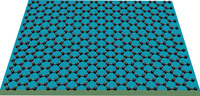 |
| Graphene consists of carbon atoms only one atomic layer thick, with the unique characteristic that its electrons behave as if they have zero mass. Image credit: Lau lab, UC Riverside. |
Abstract:
Study is first to experimentally quantify thermal contraction of graphene
UC Riverside Scientists Observe and Manipulate Ripples in Graphene, Enabling Novel Strain-Based Graphene Electronics
Riverside, CA | Posted on July 27th, 2009Graphene is nature's thinnest elastic material and displays exceptional mechanical and electronic properties. Its one-atom thickness, planar geometry, high current-carrying capacity and thermal conductivity make it ideally suited for further miniaturizing electronics through ultra-small devices and components for semiconductor circuits and computers.
But one of graphene's intrinsic features is ripples, similar to those seen on plastic wrap tightly pulled over a clamped edge. Induced by pre-existing strains in graphene, these ripples can strongly affect graphene's electronic properties, and not always favorably.
If the ripples can be controlled, however, they can be used to advantage in nanoscale devices and electronics, opening up a new arena in graphene engineering: strain-based devices.
UC Riverside's Chun Ning (Jeanie) Lau and colleagues now report the first direct observation and controlled creation of one- and two-dimensional ripples in graphene sheets. Using simple thermal manipulation, the researchers produced the ripples, and controlled their orientation, wavelength and amplitude.
"When the graphene sheets are stretched across a pair of parallel trenches, they spontaneously form nearly periodic ripples," Lau explained. "When these sheets are heated up, they actually contract, so the ripples disappear. When they are cooled down to room temperature, the ripples re-appear, with ridges at right angle to the edges of the trenches. This phenomenon is similar to what happens to a piece of thin plastic wrap that covers a container and heated in a microwave oven."
The unusual thermal contraction of graphene had been predicted theoretically, but Lau's lab is the first to demonstrate and quantify the phenomenon experimentally.
Study results appear July 26 in the advance online publication of Nature Nanotechnology.
Because graphene is both an excellent conductor and the thinnest elastic membrane, the ripples could have profound implications for graphene-based electronics.
"This is because graphene's ability to conduct electricity is expected to vary with the local shape of the membrane," Lau said. "For instance, the ripples may produce effective magnetic fields that can be used to steer and manipulate electrons in a nanoscale device without an external magnet."
Lau, an associate professor of physics and a member of UCR's Center for Nanoscale Science and Engineering, and her colleagues examined the ripples' morphology using a scanning electron microscope and an atomic force microscope. They found that almost all the graphene membranes underwent dramatic morphological changes when heated, displaying significant alterations in the ripple geometry, a buckling of the graphene membrane, or both.
Their experimental system, which involved a stage inside a scanning electron microscope (SEM) with a built-in heater, thermometer and several electrical feed-throughs, enabled them to image graphene while it was being heated and explore the interplay between graphene's mechanical, thermal and electrical properties.
"Our result has important implications for controlling thermally induced stress in graphene electronics," Lau said. "Our ability to control and manipulate the ripples in graphene sheets represents the first step towards strain-based graphene engineering. We show that suspended graphene is almost invariably rippled, and this may need to be considered in the interpretation of a broad array of existing and future research."
Proposed to supplement or replace silicon as the main electronic material, graphene is a single layer of graphite. Even though graphite has been studied for decades, the single sheet first was isolated experimentally only in 2004. Graphene's structure is a two-dimensional honeycomb lattice of carbon atoms. Structurally, it is related to carbon nanotubes (tiny hollow tubes formed by rolling up sheets of graphene) and buckyballs (hollow carbon molecules that form a closed cage).
Lau, who earlier this month was named one of the recipients of the Presidential Early Career Awards for Scientists and Engineers for the 2008 competition, joined UCR in 2004. She was joined in the 18-month study by UCR's Wenzhong Bao (first author), Feng Miao, Zhen Chen, Hang Zhang, Wanyoung Jang and Chris Dames.
The research was supported in part by grants from the National Science Foundation and the Office of Naval Research.
####
About UC Riverside
The University of California, Riverside is a doctoral research university, a living laboratory for groundbreaking exploration of issues critical to Inland Southern California, the state and communities around the world. Reflecting California's diverse culture, UCR's enrollment of about 17,000 is expected to grow to 21,000 students by 2020. The campus is planning a medical school and has reached the heart of the Coachella Valley by way of the UCR Palm Desert Graduate Center. The campus has an annual statewide economic impact of more than $1 billion. To learn more, visit www.ucr.edu or call (951) UCR-NEWS.
For more information, please click here
Contacts:
Iqbal Pittalwala
Tel: (951) 827-6050
Chun Ning (Jeanie) Lau
Copyright © UC Riverside
If you have a comment, please Contact us.Issuers of news releases, not 7th Wave, Inc. or Nanotechnology Now, are solely responsible for the accuracy of the content.
Bookmark:


| Related Links |
![]() More about Chun Ning (Jeanie) Lau
More about Chun Ning (Jeanie) Lau
![]() Department of Physics and Astronomy
Department of Physics and Astronomy
![]() Center for Nanoscale Science and Engineering
Center for Nanoscale Science and Engineering
| Related News Press |
News and information
![]() Simulating magnetization in a Heisenberg quantum spin chain April 5th, 2024
Simulating magnetization in a Heisenberg quantum spin chain April 5th, 2024
![]() NRL charters Navy�s quantum inertial navigation path to reduce drift April 5th, 2024
NRL charters Navy�s quantum inertial navigation path to reduce drift April 5th, 2024
![]() Discovery points path to flash-like memory for storing qubits: Rice find could hasten development of nonvolatile quantum memory April 5th, 2024
Discovery points path to flash-like memory for storing qubits: Rice find could hasten development of nonvolatile quantum memory April 5th, 2024
Videos/Movies
![]() New X-ray imaging technique to study the transient phases of quantum materials December 29th, 2022
New X-ray imaging technique to study the transient phases of quantum materials December 29th, 2022
![]() Solvent study solves solar cell durability puzzle: Rice-led project could make perovskite cells ready for prime time September 23rd, 2022
Solvent study solves solar cell durability puzzle: Rice-led project could make perovskite cells ready for prime time September 23rd, 2022
![]() Scientists prepare for the world�s smallest race: Nanocar Race II March 18th, 2022
Scientists prepare for the world�s smallest race: Nanocar Race II March 18th, 2022
![]() Visualizing the invisible: New fluorescent DNA label reveals nanoscopic cancer features March 4th, 2022
Visualizing the invisible: New fluorescent DNA label reveals nanoscopic cancer features March 4th, 2022
Chip Technology
![]() Discovery points path to flash-like memory for storing qubits: Rice find could hasten development of nonvolatile quantum memory April 5th, 2024
Discovery points path to flash-like memory for storing qubits: Rice find could hasten development of nonvolatile quantum memory April 5th, 2024
![]() Utilizing palladium for addressing contact issues of buried oxide thin film transistors April 5th, 2024
Utilizing palladium for addressing contact issues of buried oxide thin film transistors April 5th, 2024
![]() HKUST researchers develop new integration technique for efficient coupling of III-V and silicon February 16th, 2024
HKUST researchers develop new integration technique for efficient coupling of III-V and silicon February 16th, 2024
Nanoelectronics
![]() Interdisciplinary: Rice team tackles the future of semiconductors Multiferroics could be the key to ultralow-energy computing October 6th, 2023
Interdisciplinary: Rice team tackles the future of semiconductors Multiferroics could be the key to ultralow-energy computing October 6th, 2023
![]() Key element for a scalable quantum computer: Physicists from Forschungszentrum J�lich and RWTH Aachen University demonstrate electron transport on a quantum chip September 23rd, 2022
Key element for a scalable quantum computer: Physicists from Forschungszentrum J�lich and RWTH Aachen University demonstrate electron transport on a quantum chip September 23rd, 2022
![]() Reduced power consumption in semiconductor devices September 23rd, 2022
Reduced power consumption in semiconductor devices September 23rd, 2022
![]() Atomic level deposition to extend Moore�s law and beyond July 15th, 2022
Atomic level deposition to extend Moore�s law and beyond July 15th, 2022
Discoveries
![]() Chemical reactions can scramble quantum information as well as black holes April 5th, 2024
Chemical reactions can scramble quantum information as well as black holes April 5th, 2024
![]() New micromaterial releases nanoparticles that selectively destroy cancer cells April 5th, 2024
New micromaterial releases nanoparticles that selectively destroy cancer cells April 5th, 2024
![]() Utilizing palladium for addressing contact issues of buried oxide thin film transistors April 5th, 2024
Utilizing palladium for addressing contact issues of buried oxide thin film transistors April 5th, 2024
Announcements
![]() NRL charters Navy�s quantum inertial navigation path to reduce drift April 5th, 2024
NRL charters Navy�s quantum inertial navigation path to reduce drift April 5th, 2024
![]() Discovery points path to flash-like memory for storing qubits: Rice find could hasten development of nonvolatile quantum memory April 5th, 2024
Discovery points path to flash-like memory for storing qubits: Rice find could hasten development of nonvolatile quantum memory April 5th, 2024
|
|
||
|
|
||
| The latest news from around the world, FREE | ||
|
|
||
|
|
||
| Premium Products | ||
|
|
||
|
Only the news you want to read!
Learn More |
||
|
|
||
|
Full-service, expert consulting
Learn More |
||
|
|
||