Home > Press > Controlling the electronic surface properties of a material
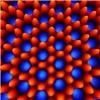 |
| A two-dimensional “electronic metamaterial” is generated by supramolecular self assembly on a metal surface. The periodic influence of the porous molecular network on the otherwise free-electron-like surface state results in the formation of an electronic band. |
Abstract:
It's commonly accepted that electrical resistance of a given material cannot be adjusted as is the case with, for example, density and color. However, Dr Meike Stöhr and her collaborators have now succeeded in developing a new method to selectively tune surface properties such as resistance.
The interdisciplinary team of physicists and chemists have developed a substance which, after heating on a copper surface, exhibits a two dimensional network with nanometer sized pores. The interaction of this network with the existing electron gas on the metal surface leads to the following effect: the electrons underneath the network are pushed into the pores to form small bunches of electrons called quantum dots.
Controlling the electronic surface properties of a material
Switzerland | Posted on July 16th, 2009Great potential for materials research
By varying parameters such as the height and diameter of the pores the possibility arises to selectively tune the properties of the material. Further possibilities arise from the ability to fill the pores with different molecules. This allows direct access to the properties of the material which are dependent on the electronic structure, such as conductivity, reflectivity and surface catalysis properties. This will lead to the emergence of new materials with adjustable electronic properties.
The underlying physical mechanisms can best be understood by a comparison of the electron-gas with waves in water. Waves on a water surface are reflected by any obstacle they meet. If the obstacle on the surface in question resembles a honeycomb structure, standing waves are set up in each cell of the honeycomb. This then leads to a wave pattern representative of the honeycomb structure of the same size and shape. "Applying this analogy to the electron gas, we see that the interaction of the network structure with the electron gas on the metal surface confines the electrons giving rise to a characteristic electron wave structure of the new material." says Stöhr.
These pore networks are good candidates for new meta-materials. These are man-made materials which, due to their period architecture, have specific optical and electronic properties not found in nature. These properties can be tuned by changing the properties of their component materials. In the case of pore networks, it is the electronic surface properties which can be tuned by careful selection of the nano-pores.
The University of Basel and the Paul Scherrer Institute are long-term partners of the Swiss Nanoscience Institute (SNI), which is also financed by the Canton of Aargau. The SNI also includes both the Nationaler Forschungsschwerpunkt Nanowissenschaften which was founded in 2001, and the Argovia-Netzwerk, founded in 2006 and also financed by the Canton of Aargau. A key partner in this project was the Swiss Light Source of the Paul Scherrer institute.
####
About Paul Scherrer Institut (PSI)
Since its founding it has developed into a successful, internationally renowned research institute for the natural and engineering sciences. This success story is due both to the professional competence, creativity and dedication of its staff, and to the financial support of the ETH Board, the Swiss Federal Council and Parliament – ultimately the Swiss taxpayers.
Education and knowledge are the most important resources in Switzerland, upon which our prosperity relies. The creation of new knowledge and the provision of high quality, internationally competitive education are goals of PSI. These goals are achieved through our own research and by supporting the work of researchers from the two ETHs in Zurich and Lausanne, universities, other research institutes and technical colleges. New knowledge creates new applications beneficial to society, promotes a competitive economy and leads to a better understanding of our world.
For more information, please click here
Contacts:
Paul Scherrer Institut
5232 Villigen PSI, Switzerland
Phone +41 (0)56 310 21 11
Fax +41 (0)56 310 21 99
Communications Officer:
Dagmar Baroke
Phone +41 (0)56 310 29 16
Copyright © Paul Scherrer Institut (PSI)
If you have a comment, please Contact us.Issuers of news releases, not 7th Wave, Inc. or Nanotechnology Now, are solely responsible for the accuracy of the content.
Bookmark:


| Related News Press |
News and information
![]() Simulating magnetization in a Heisenberg quantum spin chain April 5th, 2024
Simulating magnetization in a Heisenberg quantum spin chain April 5th, 2024
![]() NRL charters Navy’s quantum inertial navigation path to reduce drift April 5th, 2024
NRL charters Navy’s quantum inertial navigation path to reduce drift April 5th, 2024
![]() Discovery points path to flash-like memory for storing qubits: Rice find could hasten development of nonvolatile quantum memory April 5th, 2024
Discovery points path to flash-like memory for storing qubits: Rice find could hasten development of nonvolatile quantum memory April 5th, 2024
Discoveries
![]() Chemical reactions can scramble quantum information as well as black holes April 5th, 2024
Chemical reactions can scramble quantum information as well as black holes April 5th, 2024
![]() New micromaterial releases nanoparticles that selectively destroy cancer cells April 5th, 2024
New micromaterial releases nanoparticles that selectively destroy cancer cells April 5th, 2024
![]() Utilizing palladium for addressing contact issues of buried oxide thin film transistors April 5th, 2024
Utilizing palladium for addressing contact issues of buried oxide thin film transistors April 5th, 2024
Materials/Metamaterials/Magnetoresistance
![]() Nanoscale CL thermometry with lanthanide-doped heavy-metal oxide in TEM March 8th, 2024
Nanoscale CL thermometry with lanthanide-doped heavy-metal oxide in TEM March 8th, 2024
![]() Focused ion beam technology: A single tool for a wide range of applications January 12th, 2024
Focused ion beam technology: A single tool for a wide range of applications January 12th, 2024
Announcements
![]() NRL charters Navy’s quantum inertial navigation path to reduce drift April 5th, 2024
NRL charters Navy’s quantum inertial navigation path to reduce drift April 5th, 2024
![]() Discovery points path to flash-like memory for storing qubits: Rice find could hasten development of nonvolatile quantum memory April 5th, 2024
Discovery points path to flash-like memory for storing qubits: Rice find could hasten development of nonvolatile quantum memory April 5th, 2024
Quantum Dots/Rods
![]() A new kind of magnetism November 17th, 2023
A new kind of magnetism November 17th, 2023
![]() IOP Publishing celebrates World Quantum Day with the announcement of a special quantum collection and the winners of two prestigious quantum awards April 14th, 2023
IOP Publishing celebrates World Quantum Day with the announcement of a special quantum collection and the winners of two prestigious quantum awards April 14th, 2023
![]() Qubits on strong stimulants: Researchers find ways to improve the storage time of quantum information in a spin rich material January 27th, 2023
Qubits on strong stimulants: Researchers find ways to improve the storage time of quantum information in a spin rich material January 27th, 2023
![]() NIST’s grid of quantum islands could reveal secrets for powerful technologies November 18th, 2022
NIST’s grid of quantum islands could reveal secrets for powerful technologies November 18th, 2022
Research partnerships
![]() Discovery points path to flash-like memory for storing qubits: Rice find could hasten development of nonvolatile quantum memory April 5th, 2024
Discovery points path to flash-like memory for storing qubits: Rice find could hasten development of nonvolatile quantum memory April 5th, 2024
![]() Researchers’ approach may protect quantum computers from attacks March 8th, 2024
Researchers’ approach may protect quantum computers from attacks March 8th, 2024
![]() 'Sudden death' of quantum fluctuations defies current theories of superconductivity: Study challenges the conventional wisdom of superconducting quantum transitions January 12th, 2024
'Sudden death' of quantum fluctuations defies current theories of superconductivity: Study challenges the conventional wisdom of superconducting quantum transitions January 12th, 2024
|
|
||
|
|
||
| The latest news from around the world, FREE | ||
|
|
||
|
|
||
| Premium Products | ||
|
|
||
|
Only the news you want to read!
Learn More |
||
|
|
||
|
Full-service, expert consulting
Learn More |
||
|
|
||