Home > Press > IMEC launches new industrial affiliation program on GaN-on-Si technology
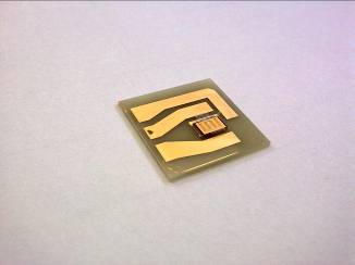 |
| IMEC's SiN/AlGaN/GaN double heterostructure field effect transistor, demonstrating breakdown voltages up to 1000V. |
Abstract:
IMEC today announces the launch of a new industrial affiliation program (IIAP) that will focus on the development of GaN technology for both power conversion and solid state lighting
applications. An important goal of the program is to lower GaN technology cost by using large-diameter GaN-on-Si and hence by leveraging on the Si scale of economics.
IMEC launches new industrial affiliation program on GaN-on-Si technology
Leuven, Belgium | Posted on July 14th, 2009The scope of the IIAP is to develop high-voltage, low-loss, high-power switching devices based on large-diameter (up to 200mm) GaN-on-Si technology. Potential applications include high-power switching in solar converters, motor drives, hybrid electrical vehicles or switch mode power supplies.
High-voltage power devices are traditionally based on Si MOSFET structures. However, for a number of applications, they are reaching intrinsic material limits. GaN-based devices can overcome these limits due to a unique combination of excellent transport properties and high electrical field operation capability. The few GaN devices today on the market are based on AlGaN/GaN high-electron mobility transistor (HEMT) structures and are normally-on devices, designed for RF applications, e.g. in wireless communication. Within the IIAP, the next-generation of power electronics
components is envisaged, requiring the development of normally-off devices (for safety reasons) with high-voltage breakdown (600-1000V) and low on-resistance, operating in enhancement mode.
A second sub-program will exploit GaN-on-Si technology for the development of high-efficiency high-power white LEDs. Key issues are enhancing the external and internal quantum efficiencies and enabling high current operation. III-nitrides in general exhibit excellent light emission properties in a very broad range of the visible and ultraviolet (UV) spectrum. However, LED illumination by these devices can only become broadly acceptable if new volume manufacturing technologies are developed that enable 150lm/W LEDs.
Common challenge for power electronics and optoelectronics is cost reduction. "GaN on large-diameter Si wafers (from 100mm and 150mm towards 200mm) in combination with CMOS compatible processes offers the best perspective to create economically viable solutions"; said Marianne Germain, GaN program director. "While very few players can today process GaN on large-diameter Si wafers, IMEC has recently shown in collaboration with AIXTRON crack-free GaN growth on 200mm wafers. Also for other challenges, the IIAP can build on IMEC's 10 years' experience in GaN technology, including unique skills in epi-layer growth, new device concept, device integration and a thin-film textured LED technology for high-efficiency III-nitride LEDs."
IMEC invites both Integrated Device Manufacturers and Compound Semiconductor Industry to join the program where they can build on IMEC's extensive expertise in GaN and benefit from a sharing of cost, risk, talent and IP.
####
About IMEC
IMEC is a world-leading independent research center in nanoelectronics and nanotechnology. IMEC vzw is headquartered in Leuven, Belgium, has a sister company in the Netherlands, IMEC-NL, offices in the US, China and Taiwan, and representatives in Japan. Its staff of more than 1650 people includes about 550 industrial residents and guest researchers. In 2008, its revenue (P&L) was EUR 270 million.
IMEC's More Moore research aims at semiconductor scaling towards sub-32nm nodes. With its More than Moore research, IMEC looks into technologies for nomadic embedded systems, wireless autonomous transducer solutions, biomedical electronics, photovoltaics, organic electronics and GaN power electronics.
IMEC's research bridges the gap between fundamental research at universities and technology development in industry. Its unique balance of processing and system know-how, intellectual property portfolio, state-of-the-art infrastructure and its strong network worldwide position IMEC as a key partner for shaping technologies for future systems.
For more information, please click here
Contacts:
Katrien Marent
IMEC Director of External Communications
T: +32 16 28 18 80
Mobile : +32 474 30 28 66,
Barbara Kalkis
Maestro Marketing & Public Relations
T: +1 408 996 9975, M: +1 408 529 4210
Copyright © IMEC
If you have a comment, please Contact us.Issuers of news releases, not 7th Wave, Inc. or Nanotechnology Now, are solely responsible for the accuracy of the content.
Bookmark:


| Related News Press |
News and information
![]() Simulating magnetization in a Heisenberg quantum spin chain April 5th, 2024
Simulating magnetization in a Heisenberg quantum spin chain April 5th, 2024
![]() NRL charters Navy�s quantum inertial navigation path to reduce drift April 5th, 2024
NRL charters Navy�s quantum inertial navigation path to reduce drift April 5th, 2024
![]() Discovery points path to flash-like memory for storing qubits: Rice find could hasten development of nonvolatile quantum memory April 5th, 2024
Discovery points path to flash-like memory for storing qubits: Rice find could hasten development of nonvolatile quantum memory April 5th, 2024
![]() Good as gold - improving infectious disease testing with gold nanoparticles April 5th, 2024
Good as gold - improving infectious disease testing with gold nanoparticles April 5th, 2024
Display technology/LEDs/SS Lighting/OLEDs
![]() Utilizing palladium for addressing contact issues of buried oxide thin film transistors April 5th, 2024
Utilizing palladium for addressing contact issues of buried oxide thin film transistors April 5th, 2024
![]() Light guide plate based on perovskite nanocomposites November 3rd, 2023
Light guide plate based on perovskite nanocomposites November 3rd, 2023
![]() Simple ballpoint pen can write custom LEDs August 11th, 2023
Simple ballpoint pen can write custom LEDs August 11th, 2023
Chip Technology
![]() Discovery points path to flash-like memory for storing qubits: Rice find could hasten development of nonvolatile quantum memory April 5th, 2024
Discovery points path to flash-like memory for storing qubits: Rice find could hasten development of nonvolatile quantum memory April 5th, 2024
![]() Utilizing palladium for addressing contact issues of buried oxide thin film transistors April 5th, 2024
Utilizing palladium for addressing contact issues of buried oxide thin film transistors April 5th, 2024
![]() HKUST researchers develop new integration technique for efficient coupling of III-V and silicon February 16th, 2024
HKUST researchers develop new integration technique for efficient coupling of III-V and silicon February 16th, 2024
Nanoelectronics
![]() Interdisciplinary: Rice team tackles the future of semiconductors Multiferroics could be the key to ultralow-energy computing October 6th, 2023
Interdisciplinary: Rice team tackles the future of semiconductors Multiferroics could be the key to ultralow-energy computing October 6th, 2023
![]() Key element for a scalable quantum computer: Physicists from Forschungszentrum J�lich and RWTH Aachen University demonstrate electron transport on a quantum chip September 23rd, 2022
Key element for a scalable quantum computer: Physicists from Forschungszentrum J�lich and RWTH Aachen University demonstrate electron transport on a quantum chip September 23rd, 2022
![]() Reduced power consumption in semiconductor devices September 23rd, 2022
Reduced power consumption in semiconductor devices September 23rd, 2022
![]() Atomic level deposition to extend Moore�s law and beyond July 15th, 2022
Atomic level deposition to extend Moore�s law and beyond July 15th, 2022
Announcements
![]() NRL charters Navy�s quantum inertial navigation path to reduce drift April 5th, 2024
NRL charters Navy�s quantum inertial navigation path to reduce drift April 5th, 2024
![]() Discovery points path to flash-like memory for storing qubits: Rice find could hasten development of nonvolatile quantum memory April 5th, 2024
Discovery points path to flash-like memory for storing qubits: Rice find could hasten development of nonvolatile quantum memory April 5th, 2024
Alliances/Trade associations/Partnerships/Distributorships
![]() Chicago Quantum Exchange welcomes six new partners highlighting quantum technology solutions, from Chicago and beyond September 23rd, 2022
Chicago Quantum Exchange welcomes six new partners highlighting quantum technology solutions, from Chicago and beyond September 23rd, 2022
![]() University of Illinois Chicago joins Brookhaven Lab's Quantum Center June 10th, 2022
University of Illinois Chicago joins Brookhaven Lab's Quantum Center June 10th, 2022
|
|
||
|
|
||
| The latest news from around the world, FREE | ||
|
|
||
|
|
||
| Premium Products | ||
|
|
||
|
Only the news you want to read!
Learn More |
||
|
|
||
|
Full-service, expert consulting
Learn More |
||
|
|
||