Home > Press > FEI Announces New Helios NanoLab 1200 Full Wafer DualBeam Solution
 |
Abstract:
Advanced DualBeam technology accelerates time to data for failure analysis, process development and process control in semiconductor and data storage manufacturing
FEI Announces New Helios NanoLab 1200 Full Wafer DualBeam Solution
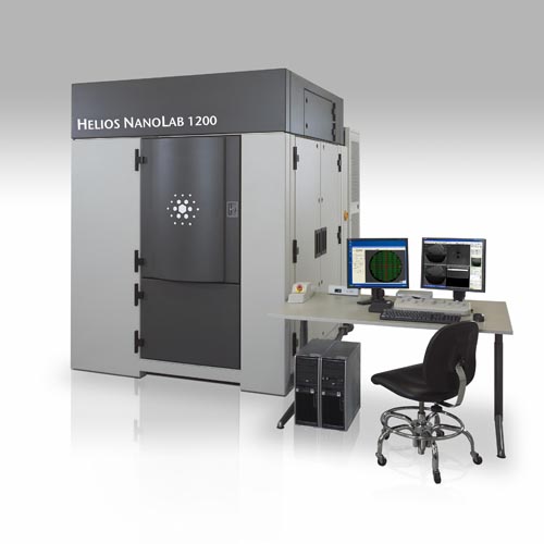
Hillsboro, OR | Posted on July 14th, 2009FEI Company (Nasdaq: FEIC), a leading provider of atomic-scale imaging and analysis systems, today announced the newest member of the Helios NanoLab(tm) Family--the Helios 1200 Full Wafer DualBeam(tm) system. The ability of the Helios 1200 to analyze full wafers up to 300 mm improves the efficiency of semiconductor and data storage failure analysis and manufacturing support labs that need to deliver accurate data quickly to the production floor.
"We've designed the new Helios 1200 DualBeam to provide the maximum productivity for failure analysis, process development and process control requirements," said Larry Dworkin, product marketing manager for FEI's full wafer systems. "The ability to introduce full wafers directly into the system allows users to navigate directly to multiple features of interest based on design data or information from other inspection and defect detection tools. Fast switching between imaging and milling permits precise, efficient control of the cross sectioning process. And imaging resolution significantly better than any other instrument in its class ensures superior analytical results."
The Helios 1200 combines world-class scanning electron microscope (SEM) image resolution and extremely fast switching between imaging and ion beam milling to deliver rapid, reliable, efficient cross-sectional analysis of structures and defects. Its ability to accommodate full wafers up to 300 mm eliminates the time required to re-establish the navigational coordinate system when working with wafer pieces.
"In the nearly two years since its introduction, our small-chamber Helios NanoLab DualBeam systems have been installed at every leading edge fab in the world," said Rudy Kellner, vice president and general manager of FEI's Electronics Division. "Now, for the first time, we can offer the same performance in a full wafer system."
When the analysis demands the higher resolution capability of a dedicated scanning transmission electron microscope (S/TEM), FEI 's Multiloader(tm) technology enables fast and secure sample transfer. FEI's new automation software product, iFAST, improves the quality and consistency of multiple, site-specific samples in a single session at a cost-per-sample that is competitive with conventional SEM bulk sample preparations. Optional energy dispersive X-ray spectrometry (EDS) on thin samples offers compositional analysis with very good spatial resolution.
The optional OmniProbe micromanipulator allows in situ extraction of prepared TEM lamella. The OmniProbe 300's new in-chamber needle exchange process eliminates the need to break chamber vacuum to obtain a new probe.
The new Helios NanoLab 1200 DualBeam system is available now.
FEI Safe Harbor Statement
This news release contains forward-looking statements that include statements regarding the performance capabilities and benefits of the Helios NanoLab 1200 DualBeam and anticipated availability date. Factors that could affect these forward-looking statements include but are not limited to failure of the product or technology to perform as expected and achieve anticipated results, unexpected technology problems and our ability to manufacture, ship and deliver the tools as expected. Please also refer to our Form 10-K, Forms 10-Q, Forms 8-K and other filings with the U.S. Securities and Exchange Commission for additional information on these factors and other factors that could cause actual results to differ materially from the forward-looking statements. FEI assumes no duty to update forward-looking statements.
####
About FEI
FEI (Nasdaq: FEIC) is a leading diversified scientific instruments company.
It is a premier provider of electron and ion-beam microscopes and tools for
nanoscale applications across many industries: industrial and academic
materials research, life sciences, semiconductors, data storage, natural
resources and more. With a 60-year history of technological innovation and
leadership, FEI has set the performance standard in transmission electron
microscopes (TEM), scanning electron microscopes (SEM) and DualBeams(tm), which
combine a SEM with a focused ion beam (FIB). FEI's imaging systems provide
3D characterization, analysis and modification/prototyping with resolutions
down to the sub-�ngstr�m (one-tenth of a nanometer) level. FEI's NanoPorts
in North America, Europe and Asia provide centers of technical excellence
where its world-class community of customers and specialists collaborate.
FEI has approximately 1800 employees and sales and service operations in
more than 50 countries around the world.
For more information, please click here
Contacts:
Sandy Fewkes, Principal (media contact)
MindWrite Communications, Inc
+1 408 224 4024
FEI Company
Fletcher Chamberlin (investors and analysts)
Investor Relations
+1 503 726 7710
Copyright © FEI Company
If you have a comment, please Contact us.Issuers of news releases, not 7th Wave, Inc. or Nanotechnology Now, are solely responsible for the accuracy of the content.
Bookmark:


| Related News Press |
News and information
![]() Simulating magnetization in a Heisenberg quantum spin chain April 5th, 2024
Simulating magnetization in a Heisenberg quantum spin chain April 5th, 2024
![]() NRL charters Navy�s quantum inertial navigation path to reduce drift April 5th, 2024
NRL charters Navy�s quantum inertial navigation path to reduce drift April 5th, 2024
![]() Discovery points path to flash-like memory for storing qubits: Rice find could hasten development of nonvolatile quantum memory April 5th, 2024
Discovery points path to flash-like memory for storing qubits: Rice find could hasten development of nonvolatile quantum memory April 5th, 2024
Chip Technology
![]() Discovery points path to flash-like memory for storing qubits: Rice find could hasten development of nonvolatile quantum memory April 5th, 2024
Discovery points path to flash-like memory for storing qubits: Rice find could hasten development of nonvolatile quantum memory April 5th, 2024
![]() Utilizing palladium for addressing contact issues of buried oxide thin film transistors April 5th, 2024
Utilizing palladium for addressing contact issues of buried oxide thin film transistors April 5th, 2024
![]() HKUST researchers develop new integration technique for efficient coupling of III-V and silicon February 16th, 2024
HKUST researchers develop new integration technique for efficient coupling of III-V and silicon February 16th, 2024
Nanoelectronics
![]() Interdisciplinary: Rice team tackles the future of semiconductors Multiferroics could be the key to ultralow-energy computing October 6th, 2023
Interdisciplinary: Rice team tackles the future of semiconductors Multiferroics could be the key to ultralow-energy computing October 6th, 2023
![]() Key element for a scalable quantum computer: Physicists from Forschungszentrum J�lich and RWTH Aachen University demonstrate electron transport on a quantum chip September 23rd, 2022
Key element for a scalable quantum computer: Physicists from Forschungszentrum J�lich and RWTH Aachen University demonstrate electron transport on a quantum chip September 23rd, 2022
![]() Reduced power consumption in semiconductor devices September 23rd, 2022
Reduced power consumption in semiconductor devices September 23rd, 2022
![]() Atomic level deposition to extend Moore�s law and beyond July 15th, 2022
Atomic level deposition to extend Moore�s law and beyond July 15th, 2022
Announcements
![]() NRL charters Navy�s quantum inertial navigation path to reduce drift April 5th, 2024
NRL charters Navy�s quantum inertial navigation path to reduce drift April 5th, 2024
![]() Discovery points path to flash-like memory for storing qubits: Rice find could hasten development of nonvolatile quantum memory April 5th, 2024
Discovery points path to flash-like memory for storing qubits: Rice find could hasten development of nonvolatile quantum memory April 5th, 2024
Tools
![]() Ferroelectrically modulate the Fermi level of graphene oxide to enhance SERS response November 3rd, 2023
Ferroelectrically modulate the Fermi level of graphene oxide to enhance SERS response November 3rd, 2023
![]() The USTC realizes In situ electron paramagnetic resonance spectroscopy using single nanodiamond sensors November 3rd, 2023
The USTC realizes In situ electron paramagnetic resonance spectroscopy using single nanodiamond sensors November 3rd, 2023
|
|
||
|
|
||
| The latest news from around the world, FREE | ||
|
|
||
|
|
||
| Premium Products | ||
|
|
||
|
Only the news you want to read!
Learn More |
||
|
|
||
|
Full-service, expert consulting
Learn More |
||
|
|
||