Home > Press > Graphene Yields Secrets to Its Extraordinary Properties
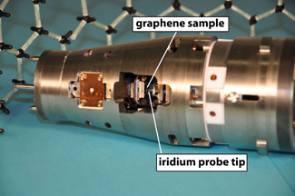 |
| NIST-built STM �shuttle� module contains the atomic-scale position-and-scan system. Graphene sample and probe tip are in the center opening. Shuttle moves between a room-temperature vacuum environment for loading to an ultracold environment for measuring. Model in background shows graphene�s honeycomb structure.
Credit: Holmes, NIST |
Abstract:
Applying innovative measurement techniques, researchers from the Georgia Institute of Technology and the National Institute of Standards and Technology (NIST) have directly measured the unusual energy spectrum of graphene, a technologically promising, two-dimensional form of carbon that has tantalized and puzzled scientists since its discovery in 2004.
Graphene Yields Secrets to Its Extraordinary Properties
Gaithersburg, MD | Posted on May 14th, 2009Published in this week's issue of Science,* their work adds new detail to help explain the unusual physical phenomena and properties associated with graphene, a single layer of carbon atoms arrayed in a repeating, honeycomb-like arrangement.
Graphene's exotic behaviors present intriguing prospects for future technologies, including high-speed, graphene-based electronics that might replace today's silicon-based integrated circuits and other devices. Even at room temperature, electrons in graphene are more than 100 times more mobile than in silicon.
Graphene apparently owes this enhanced mobility to the curious fact that its electrons and other carriers of electric charges behave as though they do not have mass. In conventional materials, the speed of electrons is related to their energy, but not in graphene. Although they do not approach the speed of light, the unbound electrons in graphene behave much like photons, massless particles of light that also move at a speed independent of their energy.
This weird massless behavior is associated with other strangeness. When ordinary conductors are put in a strong magnetic field, charge carriers such as electrons begin moving in circular orbits that are constrained to discrete, equally spaced energy levels. In graphene these levels are known to be unevenly spaced because of the "massless" electrons.
The Georgia Tech/NIST team tracked these massless electrons in action, using a specialized NIST instrument to zoom in on the graphene layer at a billion times magnification, tracking the electronic states while at the same time applying high magnetic fields. The custom-built, ultra-low-temperature and ultra-high-vacuum scanning tunneling microscope allowed them to sweep an adjustable magnetic field across graphene samples prepared at Georgia Tech, observing and mapping the peculiar non-uniform spacing among discrete energy levels that form when the material is exposed to magnetic fields.
The team developed a high-resolution map of the distribution of energy levels in graphene. In contrast to metals and other conducting materials, where the distance from one energy peak to the next is uniformly equal, this spacing is uneven in graphene.
The researchers also probed and spatially mapped graphene's hallmark "zero energy state," a curious phenomenon where the material has no electrical carriers until a magnetic field is applied.
The measurements also indicated that layers of graphene grown and then heated on a substrate of silicon-carbide behave as individual, isolated, two-dimensional sheets. On the basis of the results, the researchers suggest that graphene layers are uncoupled from adjacent layers because they stack in different rotational orientations. This finding may point the way to manufacturing methods for making large, uniform batches of graphene for a new carbon-based electronics.
The research was funded in part by the National Science Foundation.
* D.L. Miller, K.D. Kubista, G.M. Rutter, M. Ruan, W.A. de Heer, P.N. First and J.A. Stroscio. Observing the quantization of zero mass carriers in graphene. Science. May 15, 2009.
####
For more information, please click here
Contacts:
Mark Bello
(301) 975-3776
Copyright © NIST
If you have a comment, please Contact us.Issuers of news releases, not 7th Wave, Inc. or Nanotechnology Now, are solely responsible for the accuracy of the content.
Bookmark:


| Related News Press |
News and information
![]() Simulating magnetization in a Heisenberg quantum spin chain April 5th, 2024
Simulating magnetization in a Heisenberg quantum spin chain April 5th, 2024
![]() NRL charters Navy�s quantum inertial navigation path to reduce drift April 5th, 2024
NRL charters Navy�s quantum inertial navigation path to reduce drift April 5th, 2024
![]() Discovery points path to flash-like memory for storing qubits: Rice find could hasten development of nonvolatile quantum memory April 5th, 2024
Discovery points path to flash-like memory for storing qubits: Rice find could hasten development of nonvolatile quantum memory April 5th, 2024
Govt.-Legislation/Regulation/Funding/Policy
![]() NRL charters Navy�s quantum inertial navigation path to reduce drift April 5th, 2024
NRL charters Navy�s quantum inertial navigation path to reduce drift April 5th, 2024
![]() Discovery points path to flash-like memory for storing qubits: Rice find could hasten development of nonvolatile quantum memory April 5th, 2024
Discovery points path to flash-like memory for storing qubits: Rice find could hasten development of nonvolatile quantum memory April 5th, 2024
![]() Chemical reactions can scramble quantum information as well as black holes April 5th, 2024
Chemical reactions can scramble quantum information as well as black holes April 5th, 2024
Chip Technology
![]() Discovery points path to flash-like memory for storing qubits: Rice find could hasten development of nonvolatile quantum memory April 5th, 2024
Discovery points path to flash-like memory for storing qubits: Rice find could hasten development of nonvolatile quantum memory April 5th, 2024
![]() Utilizing palladium for addressing contact issues of buried oxide thin film transistors April 5th, 2024
Utilizing palladium for addressing contact issues of buried oxide thin film transistors April 5th, 2024
![]() HKUST researchers develop new integration technique for efficient coupling of III-V and silicon February 16th, 2024
HKUST researchers develop new integration technique for efficient coupling of III-V and silicon February 16th, 2024
Nanoelectronics
![]() Interdisciplinary: Rice team tackles the future of semiconductors Multiferroics could be the key to ultralow-energy computing October 6th, 2023
Interdisciplinary: Rice team tackles the future of semiconductors Multiferroics could be the key to ultralow-energy computing October 6th, 2023
![]() Key element for a scalable quantum computer: Physicists from Forschungszentrum J�lich and RWTH Aachen University demonstrate electron transport on a quantum chip September 23rd, 2022
Key element for a scalable quantum computer: Physicists from Forschungszentrum J�lich and RWTH Aachen University demonstrate electron transport on a quantum chip September 23rd, 2022
![]() Reduced power consumption in semiconductor devices September 23rd, 2022
Reduced power consumption in semiconductor devices September 23rd, 2022
![]() Atomic level deposition to extend Moore�s law and beyond July 15th, 2022
Atomic level deposition to extend Moore�s law and beyond July 15th, 2022
Discoveries
![]() Chemical reactions can scramble quantum information as well as black holes April 5th, 2024
Chemical reactions can scramble quantum information as well as black holes April 5th, 2024
![]() New micromaterial releases nanoparticles that selectively destroy cancer cells April 5th, 2024
New micromaterial releases nanoparticles that selectively destroy cancer cells April 5th, 2024
![]() Utilizing palladium for addressing contact issues of buried oxide thin film transistors April 5th, 2024
Utilizing palladium for addressing contact issues of buried oxide thin film transistors April 5th, 2024
Announcements
![]() NRL charters Navy�s quantum inertial navigation path to reduce drift April 5th, 2024
NRL charters Navy�s quantum inertial navigation path to reduce drift April 5th, 2024
![]() Discovery points path to flash-like memory for storing qubits: Rice find could hasten development of nonvolatile quantum memory April 5th, 2024
Discovery points path to flash-like memory for storing qubits: Rice find could hasten development of nonvolatile quantum memory April 5th, 2024
Research partnerships
![]() Discovery points path to flash-like memory for storing qubits: Rice find could hasten development of nonvolatile quantum memory April 5th, 2024
Discovery points path to flash-like memory for storing qubits: Rice find could hasten development of nonvolatile quantum memory April 5th, 2024
![]() Researchers� approach may protect quantum computers from attacks March 8th, 2024
Researchers� approach may protect quantum computers from attacks March 8th, 2024
![]() 'Sudden death' of quantum fluctuations defies current theories of superconductivity: Study challenges the conventional wisdom of superconducting quantum transitions January 12th, 2024
'Sudden death' of quantum fluctuations defies current theories of superconductivity: Study challenges the conventional wisdom of superconducting quantum transitions January 12th, 2024
|
|
||
|
|
||
| The latest news from around the world, FREE | ||
|
|
||
|
|
||
| Premium Products | ||
|
|
||
|
Only the news you want to read!
Learn More |
||
|
|
||
|
Full-service, expert consulting
Learn More |
||
|
|
||