Home > Press > Latest Issue of "Science": Nano-Sonar Uses Electrons to Measure under the Surface: J³lich researchers take a look deep inside metals
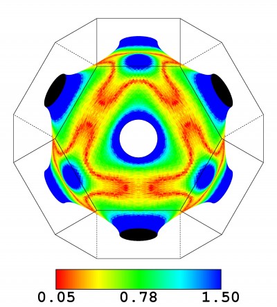 |
| The Fermi surface around a cobalt atom embedded in copper. The colours represent the curvature of the surface, which determines the reflection properties for electron waves. Image: Forschungszentrum J³lich |
Abstract:
Just as sonar sends out sound waves to explore the hidden depths of the ocean, electrons can be used by scanning tunnelling microscopes to investigate the well-hidden properties of the atomic lattice of metals. As researchers from G÷ttingen, Halle and J³lich now report in the high-impact journal "Science", they succeeded in making bulk Fermi surfaces visible in this manner. Fermi surfaces determine the most important properties of metals.
Latest Issue of "Science": Nano-Sonar Uses Electrons to Measure under the Surface: J³lich researchers take a look deep inside metals
J³lich, Germany | Posted on February 28th, 2009"Fermi surfaces give metals their personality, so to speak," explained Prof. Stefan Bl³gel, Director at the J³lich Institute of Solid State Research. Important properties, such as conductivity, heat capacity and magnetism, are determined by them. On the Fermi surfaces inside the atomic union, high-energy electrons are in motion. Depending on what form the surfaces have and what mobility is assigned to the electrons, they determine the physical properties of metals.
In their latest publication, the researchers report on how they used a scanning tunnelling microscope to direct electrons into a copper sample. As electrons spread out like waves, they pass through the metal and are scattered and reflected at obstacles in the bulk, such as single cobalt atoms. "The overlap between incoming and outgoing waves is so strong," said Dr. Samir Lounis from Forschungszentrum J³lich who turned the theoretical calculations into an experiment, "that they can be measured as spherical patterns on the surface using the scanning tunnelling microscope."
The somewhat deformed rings on the surface allow us to draw direct conclusions on the shape of the Fermi surfaces and the depth of the cobalt atoms, similar to how sonar recognises the ocean floor by means of reflected sound waves. "We hope that more sophisticated methods will make it possible to gain a detailed understanding of deep impurities and interfaces between atomic lattices," explained Lounis. For his simulations of the scanning tunnelling experiment, he used the supercomputer known as JUMP in the J³lich Supercomputing Centre.
In a related article in the "Perspectives" section of "Science", the innovative approach is praised. A scanning tunnelling microscope is primarily used to characterise the surface of a sample. Thanks to the theoretical work in J³lich, it can now be used to gain a direct insight into the bulk of solids and to understand interesting effects in the nanoworld.
Science, 27 February 2009, Vol 323, Issue 5918,
Seeing the Fermi Surface in Real Space by Nanoscale Electron Focusing, Weismann et al.
####
For more information, please click here
Contacts:
Dr. Samir Lounis
tel. +49 2461 61-6106
Prof. Stefan Bl³gel
tel. +49 2461 61-4249
Press contacts:
Kosta Schinarakis
tel. +49 2461 61-4771
Angela Wenzik
tel. +49 2461 61-6048
Copyright © Helmholtz Association
If you have a comment, please Contact us.Issuers of news releases, not 7th Wave, Inc. or Nanotechnology Now, are solely responsible for the accuracy of the content.
Bookmark:


| Related News Press |
Physics
![]() Simulating magnetization in a Heisenberg quantum spin chain April 5th, 2024
Simulating magnetization in a Heisenberg quantum spin chain April 5th, 2024
![]() Optically trapped quantum droplets of light can bind together to form macroscopic complexes March 8th, 2024
Optically trapped quantum droplets of light can bind together to form macroscopic complexes March 8th, 2024
![]() 'Sudden death' of quantum fluctuations defies current theories of superconductivity: Study challenges the conventional wisdom of superconducting quantum transitions January 12th, 2024
'Sudden death' of quantum fluctuations defies current theories of superconductivity: Study challenges the conventional wisdom of superconducting quantum transitions January 12th, 2024
News and information
![]() Simulating magnetization in a Heisenberg quantum spin chain April 5th, 2024
Simulating magnetization in a Heisenberg quantum spin chain April 5th, 2024
![]() NRL charters NavyÆs quantum inertial navigation path to reduce drift April 5th, 2024
NRL charters NavyÆs quantum inertial navigation path to reduce drift April 5th, 2024
![]() Discovery points path to flash-like memory for storing qubits: Rice find could hasten development of nonvolatile quantum memory April 5th, 2024
Discovery points path to flash-like memory for storing qubits: Rice find could hasten development of nonvolatile quantum memory April 5th, 2024
Imaging
![]() Nanoscale CL thermometry with lanthanide-doped heavy-metal oxide in TEM March 8th, 2024
Nanoscale CL thermometry with lanthanide-doped heavy-metal oxide in TEM March 8th, 2024
Discoveries
![]() Chemical reactions can scramble quantum information as well as black holes April 5th, 2024
Chemical reactions can scramble quantum information as well as black holes April 5th, 2024
![]() New micromaterial releases nanoparticles that selectively destroy cancer cells April 5th, 2024
New micromaterial releases nanoparticles that selectively destroy cancer cells April 5th, 2024
![]() Utilizing palladium for addressing contact issues of buried oxide thin film transistors April 5th, 2024
Utilizing palladium for addressing contact issues of buried oxide thin film transistors April 5th, 2024
Announcements
![]() NRL charters NavyÆs quantum inertial navigation path to reduce drift April 5th, 2024
NRL charters NavyÆs quantum inertial navigation path to reduce drift April 5th, 2024
![]() Discovery points path to flash-like memory for storing qubits: Rice find could hasten development of nonvolatile quantum memory April 5th, 2024
Discovery points path to flash-like memory for storing qubits: Rice find could hasten development of nonvolatile quantum memory April 5th, 2024
Tools
![]() Ferroelectrically modulate the Fermi level of graphene oxide to enhance SERS response November 3rd, 2023
Ferroelectrically modulate the Fermi level of graphene oxide to enhance SERS response November 3rd, 2023
![]() The USTC realizes In situ electron paramagnetic resonance spectroscopy using single nanodiamond sensors November 3rd, 2023
The USTC realizes In situ electron paramagnetic resonance spectroscopy using single nanodiamond sensors November 3rd, 2023
|
|
||
|
|
||
| The latest news from around the world, FREE | ||
|
|
||
|
|
||
| Premium Products | ||
|
|
||
|
Only the news you want to read!
Learn More |
||
|
|
||
|
Full-service, expert consulting
Learn More |
||
|
|
||