Home > Press > Lťti and Brewer Science create a common laboratory for new 3-D stacking and MEMS process flows
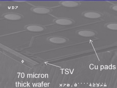 |
| 70 Ķm thick wafer with medium density TSV |
Abstract:
Lťti and Brewer Science, Inc. signed a common lab agreement to combine their expertise in integration and materials into ultra-thin wafer processing flows for 3 Dimensional Packaging using Brewer Science temporary adhesives. They are also collaborating in the development of photosensitive and non-photosensitive coatings for MEMS manufacturing processes.
Lťti and Brewer Science create a common laboratory for new 3-D stacking and MEMS process flows
Grenoble, France | Posted on February 24th, 2009A strengthened collaboration
In October 2007, Lťti and Brewer Science began the integration of WaferBondô materials into 3-D chip stacking process flows to achieve reliable, user friendly processes for ultra-thin wafer handling and processing. These products are of great interest in the creation of TSV's. At the end of 2008, the first full integration process was successfully completed. "We have, in a very limited time, achieved and characterized Unity Aspect Ratio vias on seventy microns thick wafers" says Nicolas Sillon, the Head of the Laboratory for advanced packaging and 3-D integration at Lťti. "The developed technology based on WaferBondô materials will accelerate the 3-D chip stacking projects we have at Lťti. WaferBondô materials have already been included in 3-D functional demonstrators delivered to key Lťti partners. The results we presented at the 10th Electronics Packaging Technology Conference EPTC last December in Singapore are a world premiere" he added.
"The partnership with Lťti has been extremely beneficial in achieving these successes", says Tony Flaim, Chief Technology Officer at Brewer Science, Inc. "Lťti works as a true partner, so we have jointly decided to strengthen and extend our collaboration in the framework of a 3-year, common lab." Under this agreement, leading edge Brewer Science specialty products will be used in 3-D integration and MEMS process flows.
More functionality, less space, lower cost
Focus will be on development and integration of photosensitive and non-photosensitive coatings into MEMS manufacturing processes, where high aspect ratios are mandatory, and on organic coating layers for advanced KrF and ArF photoresist processes. "Introducing advanced, tailored products will provide a very competitive advantage in the development of innovative technologies for MEMS, their packaging and their integration--the key core competencies of our department" adds Andrť Rouzaud, Deputy VP Microsystems at Lťti.
"3-D Packaging is becoming the next enabler in the industry's quest to achieve more functionality in less space for lower cost", asserts Lori Nye, Executive Director Marketing at Brewer Science. "And, new MEMS technologies provide automated interaction with the environment around us." The expanded effort between Lťti and Brewer Science in the common lab will facilitate new breakthroughs.
####
About Brewer Science
Brewer Science delivers innovative coating solutions for applications, including lithography, advanced packaging, MEMS, nanotechnology, optoelectronics and compound semiconductors. The inventor of the ARCģ (anti-reflective coatings) products for the microlithography world, we continue to expand our scope with ProTEKģ temporary etch protective coatings, WaferBONDô temporary bonding materials, and microelectronics-grade carbon nanotube solutions. Exceptional technical expertise and extensive semiconductor industry knowledge, combined with our world-class product and customer support, make Brewer Science a company that continually enhances value to the entire electronics industry.
About CEA-LETI:
CEA-LETI, the Laboratory for Electronics & Information Technology is operated by Direction de la Recherche Technologique at CEA, the French Atomic Energy Commission. It mainly aims at helping companies to increase their competitiveness through technological innovation and transfer of its technical know-how to industry. Major player in the MINATEC Micro-Nano technologies innovation center, CEA-LETI benefits from 8000 m2 state-of-the-art clean rooms, with equipment worth some 160 million euros. It is currently employing some 1600 people among whom 1100 CEA employees and co-workers of various status including 100 people from industrial partners, working in the CEA-LETI premises within the framework of bilateral collaborations. Overall, research contracts with industry are worth 75% of CEA-LETI annual income. It has a very important patents portfolio, and filed last year more than 200 patents and 700 publications. The laboratory is structured into six departments, with a specific department operating 24-7 the technological facilities of the silicon technology platform, and five program-oriented programs covering the field of microelectronics, microsystems, optronics, sytem design and telco, and technologies for bio and health. For more information, visit www.leti.fr
For more information, please click here
Contacts:
CEA-LETI
Clťment Moulet
Press Officer
Tel: +334.38.78.03.26
Brewer Science
Doyle Edwards
Marketing Communications
Tel: +1-573-364-0300
Copyright © Brewer Science
If you have a comment, please Contact us.Issuers of news releases, not 7th Wave, Inc. or Nanotechnology Now, are solely responsible for the accuracy of the content.
Bookmark:


| Related News Press |
News and information
![]() Simulating magnetization in a Heisenberg quantum spin chain April 5th, 2024
Simulating magnetization in a Heisenberg quantum spin chain April 5th, 2024
![]() NRL charters Navyís quantum inertial navigation path to reduce drift April 5th, 2024
NRL charters Navyís quantum inertial navigation path to reduce drift April 5th, 2024
![]() Discovery points path to flash-like memory for storing qubits: Rice find could hasten development of nonvolatile quantum memory April 5th, 2024
Discovery points path to flash-like memory for storing qubits: Rice find could hasten development of nonvolatile quantum memory April 5th, 2024
MEMS
Chip Technology
![]() Discovery points path to flash-like memory for storing qubits: Rice find could hasten development of nonvolatile quantum memory April 5th, 2024
Discovery points path to flash-like memory for storing qubits: Rice find could hasten development of nonvolatile quantum memory April 5th, 2024
![]() Utilizing palladium for addressing contact issues of buried oxide thin film transistors April 5th, 2024
Utilizing palladium for addressing contact issues of buried oxide thin film transistors April 5th, 2024
![]() HKUST researchers develop new integration technique for efficient coupling of III-V and silicon February 16th, 2024
HKUST researchers develop new integration technique for efficient coupling of III-V and silicon February 16th, 2024
Announcements
![]() NRL charters Navyís quantum inertial navigation path to reduce drift April 5th, 2024
NRL charters Navyís quantum inertial navigation path to reduce drift April 5th, 2024
![]() Discovery points path to flash-like memory for storing qubits: Rice find could hasten development of nonvolatile quantum memory April 5th, 2024
Discovery points path to flash-like memory for storing qubits: Rice find could hasten development of nonvolatile quantum memory April 5th, 2024
Alliances/Trade associations/Partnerships/Distributorships
![]() Chicago Quantum Exchange welcomes six new partners highlighting quantum technology solutions, from Chicago and beyond September 23rd, 2022
Chicago Quantum Exchange welcomes six new partners highlighting quantum technology solutions, from Chicago and beyond September 23rd, 2022
![]() University of Illinois Chicago joins Brookhaven Lab's Quantum Center June 10th, 2022
University of Illinois Chicago joins Brookhaven Lab's Quantum Center June 10th, 2022
|
|
||
|
|
||
| The latest news from around the world, FREE | ||
|
|
||
|
|
||
| Premium Products | ||
|
|
||
|
Only the news you want to read!
Learn More |
||
|
|
||
|
Full-service, expert consulting
Learn More |
||
|
|
||