Home > Press > Lasers achieve world record tunability
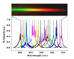 |
| Top: real color image of the nanowire wafer with color reflecting the bandgap tuning from left to right. Bottom: lasing spectra measured at 16 spots along the length of the wafer, showing spatial wavelength tunability of 200 nm. |
Abstract:
A single semiconductor laser chip with world-record wavelength tuning range of 200 nm—from 500 to 700 nm—has been demonstrated by a research team led by Cun-Zheng Ning, a professor in the Department of Electrical Engineering in the Ira A. Fulton School of Engineering at Arizona State Univ.
Lasers achieve world record tunability
Tempe, AZ | Posted on February 16th, 2009
Widely tunable semiconductor lasers offer a wide range of applications, ranging from spectroscopy, telecommunication, and on-chip biological and chemical detection. But achieving a widely tunable laser has been difficult due to limited lattice mismatch allowed in the standard epitaxial-based approach, since wavelength of light emission is determined by the bandgaps of semiconductors involved. Widely tunable lasers require alloy semiconductors with similarly tunable bandgaps, which are in turn determined by alloy composition, are usually limited by lattice mismatch with the chosen substrate.
With nanowire technology, the lattice mismatch limitation has been largely relaxed or removed completely. Thus it becomes possible in principle to grow alloy semiconductors of widely changing composition on a single substrate.
By carefully engineering and controlling the growth temperature and other parameters, the team was successful in growing ternary alloy CdSxSe1-x nanowires with composition x changing from 0 to 1 continuously from one end of the substrate to the other. As a result, the wafer has a continuous spatial grading of bandgaps between 1.75 eV and 2.5 eV, or in terms of the wavelength, between 500 and 700 nm.
Since the wafer is covered by nanowires that individually can act as nanolasers, numerous such nanolasers of continuously tuning wavelength are formed by a single growth on a single substrate. Under optical pumping, the team was able to show that each spot along the wafer length showing lasing behavior, as shown in the figure attached.
Such extremely wide tunable lasers are expected to have many potential applications. Tunable laser sources are vital elements for spectroscopic applications from research laboratories to molecular finger-print based field detection and sensing. They can act as multi-agent excitation light sources for florescence chip-based biological or chemical detections. They can also be used for multiplexing or de-multiplexing for chip-based communication applications. Many more applications can be explored, once such lasers are made electrically driven.
Ning's research group is currently working to extend the tunability to an even wider wavelength range and is developing several applications of such unique alloy materials in solar cells, detection, lighting and displays. In each of these applications, the unique materials capability is going to significantly improve the performance of the devices.
Team members include Dr. Ning's group at ASU, Dr. Anlian Pan, Weichang Zhou, Dr. Eunice Leong, Dr. Ruibin Liu, and Dr. Alan Chin, and his collaborator, Dr. B.S. Zou of Hunan University, China. For more information, contact Prof. Cun-Zheng Ning, (480) 965 7421; web: http://nanophotonics.asu.edu
The results are reported in a paper in a recent online version of the American Chemical Society journal Nano Letters. A log-in is required at pubs.acs.org.ezproxy1.lib.asu.edu/doi/full/10.1021/nl803456k
The research was supported by Science Foundation of Arizona and by US Army Research Office
####
For more information, please click here
Copyright © Arizona State University
If you have a comment, please Contact us.Issuers of news releases, not 7th Wave, Inc. or Nanotechnology Now, are solely responsible for the accuracy of the content.
Bookmark:


| Related News Press |
News and information
![]() Simulating magnetization in a Heisenberg quantum spin chain April 5th, 2024
Simulating magnetization in a Heisenberg quantum spin chain April 5th, 2024
![]() NRL charters Navy’s quantum inertial navigation path to reduce drift April 5th, 2024
NRL charters Navy’s quantum inertial navigation path to reduce drift April 5th, 2024
![]() Discovery points path to flash-like memory for storing qubits: Rice find could hasten development of nonvolatile quantum memory April 5th, 2024
Discovery points path to flash-like memory for storing qubits: Rice find could hasten development of nonvolatile quantum memory April 5th, 2024
Discoveries
![]() Chemical reactions can scramble quantum information as well as black holes April 5th, 2024
Chemical reactions can scramble quantum information as well as black holes April 5th, 2024
![]() New micromaterial releases nanoparticles that selectively destroy cancer cells April 5th, 2024
New micromaterial releases nanoparticles that selectively destroy cancer cells April 5th, 2024
![]() Utilizing palladium for addressing contact issues of buried oxide thin film transistors April 5th, 2024
Utilizing palladium for addressing contact issues of buried oxide thin film transistors April 5th, 2024
Announcements
![]() NRL charters Navy’s quantum inertial navigation path to reduce drift April 5th, 2024
NRL charters Navy’s quantum inertial navigation path to reduce drift April 5th, 2024
![]() Discovery points path to flash-like memory for storing qubits: Rice find could hasten development of nonvolatile quantum memory April 5th, 2024
Discovery points path to flash-like memory for storing qubits: Rice find could hasten development of nonvolatile quantum memory April 5th, 2024
Photonics/Optics/Lasers
![]() With VECSELs towards the quantum internet Fraunhofer: IAF achieves record output power with VECSEL for quantum frequency converters April 5th, 2024
With VECSELs towards the quantum internet Fraunhofer: IAF achieves record output power with VECSEL for quantum frequency converters April 5th, 2024
![]() Nanoscale CL thermometry with lanthanide-doped heavy-metal oxide in TEM March 8th, 2024
Nanoscale CL thermometry with lanthanide-doped heavy-metal oxide in TEM March 8th, 2024
![]() Optically trapped quantum droplets of light can bind together to form macroscopic complexes March 8th, 2024
Optically trapped quantum droplets of light can bind together to form macroscopic complexes March 8th, 2024
![]() HKUST researchers develop new integration technique for efficient coupling of III-V and silicon February 16th, 2024
HKUST researchers develop new integration technique for efficient coupling of III-V and silicon February 16th, 2024
|
|
||
|
|
||
| The latest news from around the world, FREE | ||
|
|
||
|
|
||
| Premium Products | ||
|
|
||
|
Only the news you want to read!
Learn More |
||
|
|
||
|
Full-service, expert consulting
Learn More |
||
|
|
||