Home > Press > Carbon nanotube avalanche process nearly doubles current
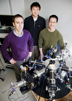 |
| Photo by L. Brian Stauffer Electrical and computer engineering professor Eric Pop, from left, worked with undergraduate Yang Zhao and graduate student Albert Liao, both in ECE, to demonstrate a remarkable increase in the current-carrying capacity of carbon nanotubes. |
Abstract:
By pushing carbon nanotubes close to their breaking point, researchers at the University of Illinois have demonstrated a remarkable increase in the current-carrying capacity of the nanotubes, well beyond what was previously thought possible.
Carbon nanotube avalanche process nearly doubles current
Champaign, IL | Posted on February 9th, 2009The researchers drove semiconducting carbon nanotubes into an avalanche process that carries more electrons down more paths, similar to the way a multilane highway carries more traffic than a one-lane road.
"Single-wall carbon nanotubes are already known to carry current densities up to 100 times higher than the best metals like copper," said Eric Pop, a professor of electrical and computer engineering at the U. of I. "We now show that semiconducting nanotubes can carry nearly twice as much current as previously thought."
As reported in the journal Physical Review Letters, the researchers found that at high electric fields (10 volts per micron), energetic electrons and holes can create additional electron-hole pairs, leading to an avalanche effect where the free carriers multiply and the current rapidly increases until the nanotube breaks down.
The sharp increase in current, Pop said, is due to the onset of avalanche impact ionization, a phenomenon observed in certain semiconductor diodes and transistors at high electric fields, but not previously seen in nanotubes.
While the maximum current carrying capacity for metallic nanotubes has been measured at about 25 microamps, the maximum current carrying capacity for semiconducting nanotubes is less established. Previous theoretical predictions suggested a similar limit for single-band conduction in semiconducting nanotubes.
To study current behavior, Pop, graduate student Albert Liao and undergraduate student Yang Zhao first grew single-wall carbon nanotubes by chemical vapor deposition from a patterned iron catalyst. Palladium contacts were used for measurement purposes. The researchers then pushed the nanotubes close to their breaking point in an oxygen-free environment.
"We found that the current first plateaus near 25 microamps, and then sharply increases at higher electric fields," said Pop, who also is affiliated with the Beckman Institute and the Micro and Nanotechnology Laboratory at the U. of I. "We performed repeated measurements, obtaining currents of up to 40 microamps, nearly twice those of previous reports."
By inducing very high electric fields in the nanotubes, the researchers drove some of the charge carriers into nearby subbands, as part of the avalanche process. Instead of being in just one "lane," the electrons and holes could occupy several available lanes, resulting in much greater current.
The avalanche process (which cannot be observed in metallic carbon nanotubes because an energy gap is required for electron-hole multiplication) offers additional functionality to semiconducting nanotubes, Pop said. "Our results suggest that avalanche-driven devices with highly nonlinear turn-on characteristics can be fashioned from semiconducting single wall nanotubes."
Funding was provided by the National Science Foundation and the National Institute of Standards and Technology through the Nanoelectronics Research Initiative.
####
For more information, please click here
Contacts:
James E. Kloeppel
Physical Sciences Editor
217-244-1073
Eric Pop
217-244-2070
Copyright © University of Illinois at Urbana-Champaign
If you have a comment, please Contact us.Issuers of news releases, not 7th Wave, Inc. or Nanotechnology Now, are solely responsible for the accuracy of the content.
Bookmark:


| Related News Press |
News and information
![]() Simulating magnetization in a Heisenberg quantum spin chain April 5th, 2024
Simulating magnetization in a Heisenberg quantum spin chain April 5th, 2024
![]() NRL charters Navy�s quantum inertial navigation path to reduce drift April 5th, 2024
NRL charters Navy�s quantum inertial navigation path to reduce drift April 5th, 2024
![]() Discovery points path to flash-like memory for storing qubits: Rice find could hasten development of nonvolatile quantum memory April 5th, 2024
Discovery points path to flash-like memory for storing qubits: Rice find could hasten development of nonvolatile quantum memory April 5th, 2024
Govt.-Legislation/Regulation/Funding/Policy
![]() NRL charters Navy�s quantum inertial navigation path to reduce drift April 5th, 2024
NRL charters Navy�s quantum inertial navigation path to reduce drift April 5th, 2024
![]() Discovery points path to flash-like memory for storing qubits: Rice find could hasten development of nonvolatile quantum memory April 5th, 2024
Discovery points path to flash-like memory for storing qubits: Rice find could hasten development of nonvolatile quantum memory April 5th, 2024
![]() Chemical reactions can scramble quantum information as well as black holes April 5th, 2024
Chemical reactions can scramble quantum information as well as black holes April 5th, 2024
Chip Technology
![]() Discovery points path to flash-like memory for storing qubits: Rice find could hasten development of nonvolatile quantum memory April 5th, 2024
Discovery points path to flash-like memory for storing qubits: Rice find could hasten development of nonvolatile quantum memory April 5th, 2024
![]() Utilizing palladium for addressing contact issues of buried oxide thin film transistors April 5th, 2024
Utilizing palladium for addressing contact issues of buried oxide thin film transistors April 5th, 2024
![]() HKUST researchers develop new integration technique for efficient coupling of III-V and silicon February 16th, 2024
HKUST researchers develop new integration technique for efficient coupling of III-V and silicon February 16th, 2024
Nanotubes/Buckyballs/Fullerenes/Nanorods/Nanostrings
![]() Tests find no free-standing nanotubes released from tire tread wear September 8th, 2023
Tests find no free-standing nanotubes released from tire tread wear September 8th, 2023
![]() Detection of bacteria and viruses with fluorescent nanotubes July 21st, 2023
Detection of bacteria and viruses with fluorescent nanotubes July 21st, 2023
Nanoelectronics
![]() Interdisciplinary: Rice team tackles the future of semiconductors Multiferroics could be the key to ultralow-energy computing October 6th, 2023
Interdisciplinary: Rice team tackles the future of semiconductors Multiferroics could be the key to ultralow-energy computing October 6th, 2023
![]() Key element for a scalable quantum computer: Physicists from Forschungszentrum J�lich and RWTH Aachen University demonstrate electron transport on a quantum chip September 23rd, 2022
Key element for a scalable quantum computer: Physicists from Forschungszentrum J�lich and RWTH Aachen University demonstrate electron transport on a quantum chip September 23rd, 2022
![]() Reduced power consumption in semiconductor devices September 23rd, 2022
Reduced power consumption in semiconductor devices September 23rd, 2022
![]() Atomic level deposition to extend Moore�s law and beyond July 15th, 2022
Atomic level deposition to extend Moore�s law and beyond July 15th, 2022
Discoveries
![]() Chemical reactions can scramble quantum information as well as black holes April 5th, 2024
Chemical reactions can scramble quantum information as well as black holes April 5th, 2024
![]() New micromaterial releases nanoparticles that selectively destroy cancer cells April 5th, 2024
New micromaterial releases nanoparticles that selectively destroy cancer cells April 5th, 2024
![]() Utilizing palladium for addressing contact issues of buried oxide thin film transistors April 5th, 2024
Utilizing palladium for addressing contact issues of buried oxide thin film transistors April 5th, 2024
Announcements
![]() NRL charters Navy�s quantum inertial navigation path to reduce drift April 5th, 2024
NRL charters Navy�s quantum inertial navigation path to reduce drift April 5th, 2024
![]() Discovery points path to flash-like memory for storing qubits: Rice find could hasten development of nonvolatile quantum memory April 5th, 2024
Discovery points path to flash-like memory for storing qubits: Rice find could hasten development of nonvolatile quantum memory April 5th, 2024
|
|
||
|
|
||
| The latest news from around the world, FREE | ||
|
|
||
|
|
||
| Premium Products | ||
|
|
||
|
Only the news you want to read!
Learn More |
||
|
|
||
|
Full-service, expert consulting
Learn More |
||
|
|
||