Home > Press > Applied Materials’ New Enabler E5 System Solves Critical Contact Etch Challenges for 32nm Memory Chips
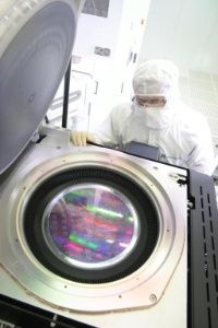 |
| The Applied Centura Enabler E5 sets an industry benchmark, enabling customers to etch 40:1 high aspect ratio contacts with the excellent profile control required for 32nm and below memory chip manufacturing. (Photo: Business Wire) |
Abstract:
Applied Materials, Inc. today unveiled its Applied Centura® Enabler® E5 dielectric etch system, the industry's most advanced solution for creating the 40:1 high aspect ratio contact features that are critical to the yield and performance of 32nm and below DRAM and Flash memory chips. The Enabler E5 sets a new benchmark in profile control, enabling customers to manufacture high performance, robust, next-generation memory devices with >80% bottom-to-top CD ratios across the wafer, and with less than 3nm bowing of the contact sidewall.
Applied Materials’ New Enabler E5 System Solves Critical Contact Etch Challenges for 32nm Memory Chips
SANTA CLARA, CA | Posted on December 3rd, 2008 "Next-generation Flash and DRAM devices pose a significant challenge for dielectric etch systems since it is very difficult to achieve the global profile control necessary for fabricating high aspect ratio contacts," said Ellie Yieh, vice president and general manager of Applied Materials' Etch and Cleans Business Unit. "The Enabler E5 is the only system that can meet all these requirements, allowing memory manufacturers to continue to increase density and reduce the cost-per-bit."
"Customers are very excited about the Enabler E5 system's exceptional profile control," added Ms. Yieh. "We're seeing strong demand for this product with multiple systems installed worldwide and repeat orders from leading memory manufacturers where it has solidly won multiple head-to-head run-offs with other systems."
Central to the Enabler E5 system's performance are its unique reactor architecture and precise process control that provide repeatable, uniform vertical profiles at high aspect ratios globally - from edge-to-edge and wafer-to-wafer - addressing a critical yield inhibitor at higher memory densities. The proprietary chamber technology also provides more efficient cleaning, delivering 50% longer between-maintenance intervals than any competitive system. For more information on the Applied Centura Enabler E5 system, please visit:
www.appliedmaterials.com/products/dielectric_etch_enabler_4.html.
####
About Applied Materials, Inc.
Applied Materials, Inc. (Nasdaq:AMAT) is the global leader in Nanomanufacturing Technology™ solutions with a broad portfolio of innovative equipment, service and software products for the fabrication of semiconductor chips, flat panel displays, solar photovoltaic cells, flexible electronics and energy efficient glass. At Applied Materials, we apply Nanomanufacturing Technology to improve the way people live.
For more information, please click here
Contacts:
Applied Materials, Inc.
Betty Newboe
408-563-0647 (editorial/media)
Robert Friess
408-986-7977 (financial community)
Copyright © Business Wire 2008
If you have a comment, please Contact us.Issuers of news releases, not 7th Wave, Inc. or Nanotechnology Now, are solely responsible for the accuracy of the content.
Bookmark:


| Related News Press |
News and information
![]() Simulating magnetization in a Heisenberg quantum spin chain April 5th, 2024
Simulating magnetization in a Heisenberg quantum spin chain April 5th, 2024
![]() NRL charters Navy’s quantum inertial navigation path to reduce drift April 5th, 2024
NRL charters Navy’s quantum inertial navigation path to reduce drift April 5th, 2024
![]() Discovery points path to flash-like memory for storing qubits: Rice find could hasten development of nonvolatile quantum memory April 5th, 2024
Discovery points path to flash-like memory for storing qubits: Rice find could hasten development of nonvolatile quantum memory April 5th, 2024
Chip Technology
![]() Discovery points path to flash-like memory for storing qubits: Rice find could hasten development of nonvolatile quantum memory April 5th, 2024
Discovery points path to flash-like memory for storing qubits: Rice find could hasten development of nonvolatile quantum memory April 5th, 2024
![]() Utilizing palladium for addressing contact issues of buried oxide thin film transistors April 5th, 2024
Utilizing palladium for addressing contact issues of buried oxide thin film transistors April 5th, 2024
![]() HKUST researchers develop new integration technique for efficient coupling of III-V and silicon February 16th, 2024
HKUST researchers develop new integration technique for efficient coupling of III-V and silicon February 16th, 2024
Announcements
![]() NRL charters Navy’s quantum inertial navigation path to reduce drift April 5th, 2024
NRL charters Navy’s quantum inertial navigation path to reduce drift April 5th, 2024
![]() Discovery points path to flash-like memory for storing qubits: Rice find could hasten development of nonvolatile quantum memory April 5th, 2024
Discovery points path to flash-like memory for storing qubits: Rice find could hasten development of nonvolatile quantum memory April 5th, 2024
Tools
![]() Ferroelectrically modulate the Fermi level of graphene oxide to enhance SERS response November 3rd, 2023
Ferroelectrically modulate the Fermi level of graphene oxide to enhance SERS response November 3rd, 2023
![]() The USTC realizes In situ electron paramagnetic resonance spectroscopy using single nanodiamond sensors November 3rd, 2023
The USTC realizes In situ electron paramagnetic resonance spectroscopy using single nanodiamond sensors November 3rd, 2023
|
|
||
|
|
||
| The latest news from around the world, FREE | ||
|
|
||
|
|
||
| Premium Products | ||
|
|
||
|
Only the news you want to read!
Learn More |
||
|
|
||
|
Full-service, expert consulting
Learn More |
||
|
|
||