Home > Press > Forced to insulate: Substrate-induced strain can be used to switch an organic superconductor into an insulator that responds to the application of a v
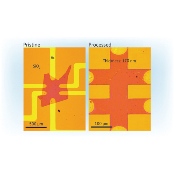 |
| Figure 1: Images of the device investigated. The left panel shows a κ-Br single crystal film deposited on a SiO2/Si substrate with pre-patterned gold contacts. The right panel shows the same device after a pulsed laser has been used to shape the κ-Br crystal into a more regular geometry. |
Abstract:
Scientists at the RIKEN Advanced Science Institute, Wako, Saitama University, Saitama, and the National Institute of Advanced Industrial Science and Technology, Tsukuba, have demonstrated that an organic film can be switched from being a superconductor to an insulator through the proper choice of substrate1. In addition, the researchers have shown that the electrical conductivity of the film can be tuned by an external voltage, which is necessary to realize transistors.
Forced to insulate: Substrate-induced strain can be used to switch an organic superconductor into an insulator that responds to the application of a v
Japan | Posted on October 25th, 2008When the film of a molecular conductor is deposited on a substrate of an organic electronic device, considerable strain can arise that dramatically affects its transport properties, particularly when the temperature varies owing to differences in thermal contraction between film and substrate.
In demonstrating the switch from superconductor to insulator, Yoshitaka Kawasugi and colleagues focussed on the well-known organic superconductor κ-(BEDT-TTF)2Cu[N(CN)2]Br�κ-Br in short�that has a 2.93% thermal contraction when cooled from room temperature (~300 K) to 20 K. At room temperature, the material is an insulator, but when cooled it becomes a metal at approximately 50 K, and eventually a superconductor at 11 K.
The researchers examined the κ-Br film deposited on a silicon-based (SiO2/Si) substrate (Fig. 1), which is nominally unshrinkable and therefore hinders thermal contraction. Their transport measurements show that resistance increases with decreasing temperature, from 300 K to below 10 K, which means that the silicon-based substrate has made the film an insulator throughout this temperature range.
To explain these results, Kawasugi and colleagues compared the effect of the non-shrinking substrate with that of pressure. Using a phase diagram of compounds similar to κ-Br, the researchers assumed that although the material is a superconductor below 11 K at ambient pressure, it becomes an insulator when negative pressure is applied. By hindering thermal contraction, the SiO2/Si substrate has the same effect as negative pressure, so when the sample is cooled, the pressure effectively decreases, and the sample stays insulating.
Kawasugi and colleagues also verified that the strain-induced insulator exhibits a field effect, which is variable conductance with an applied gate voltage. As Kawasugi explains, "The gate voltage applied to the film enhanced its conductivity by several orders of magnitude, and the field-effect mobility reached a very high value as an organic transistor, 94 cm2/Vs at low temperature." From the phase diagram, the insulating film is in the proximity of the superconducting phase, and with even higher gate voltages it may switch to a superconductor. "The results open the way to field-induced superconductivity in organic materials," says Kawasugi.
Reference
1. Kawasugi, Y., Yamamoto, H.M., Hosoda, M., Tajima, N., Fukunaga, T., Tsukagoshi, K. & Kato, R. Strain-induced superconductor/insulator transition and field effect in a thin single crystal of molecular conductor. Applied Physics Letters 92, 243508 (2008).
The corresponding author for this highlight is based at the RIKEN Condensed Molecular Materials Laboratory
####
For more information, please click here
Copyright © Riken
If you have a comment, please Contact us.Issuers of news releases, not 7th Wave, Inc. or Nanotechnology Now, are solely responsible for the accuracy of the content.
Bookmark:


| Related Links |
| Related News Press |
News and information
![]() Simulating magnetization in a Heisenberg quantum spin chain April 5th, 2024
Simulating magnetization in a Heisenberg quantum spin chain April 5th, 2024
![]() NRL charters Navy�s quantum inertial navigation path to reduce drift April 5th, 2024
NRL charters Navy�s quantum inertial navigation path to reduce drift April 5th, 2024
![]() Discovery points path to flash-like memory for storing qubits: Rice find could hasten development of nonvolatile quantum memory April 5th, 2024
Discovery points path to flash-like memory for storing qubits: Rice find could hasten development of nonvolatile quantum memory April 5th, 2024
Chip Technology
![]() Discovery points path to flash-like memory for storing qubits: Rice find could hasten development of nonvolatile quantum memory April 5th, 2024
Discovery points path to flash-like memory for storing qubits: Rice find could hasten development of nonvolatile quantum memory April 5th, 2024
![]() Utilizing palladium for addressing contact issues of buried oxide thin film transistors April 5th, 2024
Utilizing palladium for addressing contact issues of buried oxide thin film transistors April 5th, 2024
![]() HKUST researchers develop new integration technique for efficient coupling of III-V and silicon February 16th, 2024
HKUST researchers develop new integration technique for efficient coupling of III-V and silicon February 16th, 2024
Discoveries
![]() Chemical reactions can scramble quantum information as well as black holes April 5th, 2024
Chemical reactions can scramble quantum information as well as black holes April 5th, 2024
![]() New micromaterial releases nanoparticles that selectively destroy cancer cells April 5th, 2024
New micromaterial releases nanoparticles that selectively destroy cancer cells April 5th, 2024
![]() Utilizing palladium for addressing contact issues of buried oxide thin film transistors April 5th, 2024
Utilizing palladium for addressing contact issues of buried oxide thin film transistors April 5th, 2024
Announcements
![]() NRL charters Navy�s quantum inertial navigation path to reduce drift April 5th, 2024
NRL charters Navy�s quantum inertial navigation path to reduce drift April 5th, 2024
![]() Discovery points path to flash-like memory for storing qubits: Rice find could hasten development of nonvolatile quantum memory April 5th, 2024
Discovery points path to flash-like memory for storing qubits: Rice find could hasten development of nonvolatile quantum memory April 5th, 2024
|
|
||
|
|
||
| The latest news from around the world, FREE | ||
|
|
||
|
|
||
| Premium Products | ||
|
|
||
|
Only the news you want to read!
Learn More |
||
|
|
||
|
Full-service, expert consulting
Learn More |
||
|
|
||