Home > Press > Critical questions: Ripples in the structure of graphene could be the key to understanding its unusual characteristics
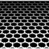 |
| Figure 1: Graphene consists of a single layer of carbon atoms arranged in a hexagonal array. Its structure and two-dimensional nature gives rise to its unique and potentially useful electronic characteristics.
source: Wikimedia/Thomas Szkopek |
Abstract:
Graphene is a two-dimensional material that consists of a hexagonal array of carbon just one atom thick (Fig. 1). Although it is essentially just a single sheet of graphite, its properties are remarkable and unique. Notably, its charge carriers behave like massless relativistic particles, and move at a speed of just 300 times less than the speed of light—many times more quickly than in silicon. This makes graphene a potentially attractive alternative to silicon as future computer chips.
Critical questions: Ripples in the structure of graphene could be the key to understanding its unusual characteristics
Japan | Posted on October 19th, 2008Many questions remain about graphene. A numerical study conducted by an international team of physicists including Akira Furusaki of RIKEN's Advanced Science Institute in Wako, attempts to explain the unusual quantum Hall effect that arises in graphene, and the influence of disorder of its 2D structure on its behavior1.
The quantum Hall effect occurs in metal-like systems whose electrons are confined to move only in a two-dimensional plane. It is characterized by the emergence of plateaus in the conductance measured transverse to the flow of current through the system—known as the Hall conductance—when a large magnetic field is applied through the plane.
In graphene, the quantum Hall effect is subtly different to that in other 2D systems. Normally, the Hall conductance begins at zero and increases in exact increments, described as e2/h, with increasing magnetic field or charge concentration. In graphene, however, the conductance changes in multiples of 4e2/h and the whole characteristic is shifted by half this value.
Moreover, in most systems it is usually destroyed by disorder or by thermal fluctuations at temperatures much above absolute zero. But in graphene, it is remarkably insensitive to both, with the Hall plateaus around zero conductivity evident all the way up to room temperature.
The simulations performed by Furusaki and colleagues suggest that the robustness of the quantum Hall effect in graphene arises as a result of the relativistic nature of its charge carriers. Under certain amounts of disorder, the wavefunctions of zero-energy carrier states do not become localized in the same way as those of nonrelativistic carriers in conventional quantum Hall systems would. The researchers argue that the occurrence of such nonlocalized states—known as critical states—could explain why the initial Hall plateaus occur at +/- 2e2/h, rather than at zero before increasing in multiples of 4e2/h. Moreover, they argue that the expected occurrence of ripples in graphene's structure could be enough to cause these nonlocalized states to emerge.
Reference
1. Nomura, K., Ryu, S., Koshino, M., Mudry, C. & Furusaki, A. Quantum Hall effect of massless Dirac fermions in a vanishing magnetic field. Physical Review Letters 100, 246806 (2008).
The corresponding author for this highlight is based at the RIKEN Condensed Matter Theory Laboratory
####
For more information, please click here
Copyright © Riken
If you have a comment, please Contact us.Issuers of news releases, not 7th Wave, Inc. or Nanotechnology Now, are solely responsible for the accuracy of the content.
Bookmark:


| Related Links |
| Related News Press |
News and information
![]() Simulating magnetization in a Heisenberg quantum spin chain April 5th, 2024
Simulating magnetization in a Heisenberg quantum spin chain April 5th, 2024
![]() NRL charters Navy’s quantum inertial navigation path to reduce drift April 5th, 2024
NRL charters Navy’s quantum inertial navigation path to reduce drift April 5th, 2024
![]() Discovery points path to flash-like memory for storing qubits: Rice find could hasten development of nonvolatile quantum memory April 5th, 2024
Discovery points path to flash-like memory for storing qubits: Rice find could hasten development of nonvolatile quantum memory April 5th, 2024
Chip Technology
![]() Discovery points path to flash-like memory for storing qubits: Rice find could hasten development of nonvolatile quantum memory April 5th, 2024
Discovery points path to flash-like memory for storing qubits: Rice find could hasten development of nonvolatile quantum memory April 5th, 2024
![]() Utilizing palladium for addressing contact issues of buried oxide thin film transistors April 5th, 2024
Utilizing palladium for addressing contact issues of buried oxide thin film transistors April 5th, 2024
![]() HKUST researchers develop new integration technique for efficient coupling of III-V and silicon February 16th, 2024
HKUST researchers develop new integration technique for efficient coupling of III-V and silicon February 16th, 2024
Discoveries
![]() Chemical reactions can scramble quantum information as well as black holes April 5th, 2024
Chemical reactions can scramble quantum information as well as black holes April 5th, 2024
![]() New micromaterial releases nanoparticles that selectively destroy cancer cells April 5th, 2024
New micromaterial releases nanoparticles that selectively destroy cancer cells April 5th, 2024
![]() Utilizing palladium for addressing contact issues of buried oxide thin film transistors April 5th, 2024
Utilizing palladium for addressing contact issues of buried oxide thin film transistors April 5th, 2024
Announcements
![]() NRL charters Navy’s quantum inertial navigation path to reduce drift April 5th, 2024
NRL charters Navy’s quantum inertial navigation path to reduce drift April 5th, 2024
![]() Discovery points path to flash-like memory for storing qubits: Rice find could hasten development of nonvolatile quantum memory April 5th, 2024
Discovery points path to flash-like memory for storing qubits: Rice find could hasten development of nonvolatile quantum memory April 5th, 2024
Quantum nanoscience
![]() Simulating magnetization in a Heisenberg quantum spin chain April 5th, 2024
Simulating magnetization in a Heisenberg quantum spin chain April 5th, 2024
![]() Optically trapped quantum droplets of light can bind together to form macroscopic complexes March 8th, 2024
Optically trapped quantum droplets of light can bind together to form macroscopic complexes March 8th, 2024
![]() Bridging light and electrons January 12th, 2024
Bridging light and electrons January 12th, 2024
![]() 'Sudden death' of quantum fluctuations defies current theories of superconductivity: Study challenges the conventional wisdom of superconducting quantum transitions January 12th, 2024
'Sudden death' of quantum fluctuations defies current theories of superconductivity: Study challenges the conventional wisdom of superconducting quantum transitions January 12th, 2024
|
|
||
|
|
||
| The latest news from around the world, FREE | ||
|
|
||
|
|
||
| Premium Products | ||
|
|
||
|
Only the news you want to read!
Learn More |
||
|
|
||
|
Full-service, expert consulting
Learn More |
||
|
|
||