Home > Press > Scientists Engineer Superconducting Thin Films: One step closer to fabrication of useful devices such as superconductive transistors
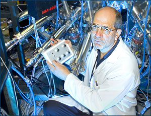 |
| Ivan Bozovic |
Abstract:
One major goal on the path toward making useful superconducting devices has been engineering materials that act as superconductors at the nanoscale — the realm of billionths of a meter. Such nanoscale superconductors would be useful in devices such as superconductive transistors and eventually in ultrafast, power-saving electronics.
Scientists Engineer Superconducting Thin Films: One step closer to fabrication of useful devices such as superconductive transistors
UPTON, NY | Posted on October 8th, 2008In the October 9, 2008, issue of Nature, scientists at the U.S. Department of Energy's (DOE) Brookhaven National Laboratory report that they have successfully produced two-layer thin films where neither layer is superconducting on its own, but which exhibit a nanometer-thick region of superconductivity at their interface. Furthermore, they demonstrate the ability to elevate the temperature of superconductivity at this interface to temperatures exceeding 50 kelvin (-370°F), a relatively high temperature deemed more practical for real-world devices.
"This work provides definitive proof of our ability to produce robust superconductivity at the interface of two layers confined within an extremely thin, 1-2-nanometer-thick layer near the physical boundary between the two materials," said physicist Ivan Bozovic, who leads the Brookhaven thin film research team. "It opens vistas for further progress, including using these techniques to significantly enhance superconducting properties in other known or new superconductors."
Bozovic foresees future research investigating different combinations of non-superconducting materials. "Further study of the temperature-enhancement mechanism might even tell us something about the big puzzle — the mechanism underlying high-temperature superconductivity, which remains one of the most important open problems in condensed matter physics," he said.
Bozovic's team had reported in 2002 the bizarre observation that the critical temperature — the temperature below which the sample superconducts — could be enhanced by as much as 25 percent in bilayers of two dissimilar copper-based materials. However, at that time, the scientists had no understanding of what caused this enhancement and in which part of the sample the superconductivity was located.
To investigate this further, they synthesized more than 200 single-phase, bilayer and trilayer films with insulating, metallic, and superconducting blocks in all possible combinations and of varying layer thickness. The films were grown in a unique atomic-layer-by-layer molecular beam epitaxy system designed and built by Bozovic and coworkers to enable the synthesis of atomically smooth films as well as multilayers with perfect interfaces. "The greatest technical challenge was to prove convincingly that the superconducting effect does not come from simple mixing of the two materials and formation of a third, chemically and physically distinct layer between the two constituent layers," Bozovic said. Collaborators at Cornell University ruled out this possibility using atomic-resolution transmission electron microscopy to identify the samples' constituent chemical elements, proving that the layers indeed remained distinct.
"It is too early to tell what applications this research might yield," Bozovic said, "but already at this stage we can speculate that this brings us one big step closer to fabrication of useful three-terminal superconducting devices, such as a superconductive field-effect transistor." In such a device, one would be able to switch the transistor from the superconducting to the resistive state by means of an external electric field, controlled by applying a voltage and using the third (gate) electrode. Circuits built from such devices would be much faster and use less power than the current ones based on semiconductors.
"No matter what the applications, this work is a nice demonstration of our ability to engineer and control materials at sub-nanometer scale, with designed and enhanced functionality," Bozovic said.
The Brookhaven scientists have filed a U.S. provisional patent application for this work. For information about licensing, please contact Kimberley Elcess, 631-344-4151,
In addition to Bozovic, the research team includes Adrian Gozar, Gennady Logvenov, and Anthony Bollinger of Brookhaven Lab, Lenna Fitting Kourkoutis and David A. Muller of Cornell University, and Lucille A. Giannuzzi of the FEI Company, Hillsboro, Oregon. The research at Brookhaven Lab was funded by the Office of Basic Energy Sciences within the DOE's Office of Science; the Cornell work was funded by the Office of Naval Research.
####
About Brookhaven National Laboratory
One of ten national laboratories overseen and primarily funded by the Office of Science of the U.S. Department of Energy (DOE), Brookhaven National Laboratory conducts research in the physical, biomedical, and environmental sciences, as well as in energy technologies and national security. Brookhaven Lab also builds and operates major scientific facilities available to university, industry and government researchers. Brookhaven is operated and managed for DOE’s Office of Science by Brookhaven Science Associates, a limited-liability company founded by Stony Brook University, the largest academic user of Laboratory facilities, and Battelle, a nonprofit, applied science and technology organization.
For more information, please click here
Contacts:
Karen McNulty Walsh
(631) 344-8350
or
Mona S. Rowe
(631) 344-5056
Copyright © Brookhaven National Laboratory
If you have a comment, please Contact us.Issuers of news releases, not 7th Wave, Inc. or Nanotechnology Now, are solely responsible for the accuracy of the content.
Bookmark:


| Related News Press |
Physics
![]() Simulating magnetization in a Heisenberg quantum spin chain April 5th, 2024
Simulating magnetization in a Heisenberg quantum spin chain April 5th, 2024
![]() Nanoscale CL thermometry with lanthanide-doped heavy-metal oxide in TEM March 8th, 2024
Nanoscale CL thermometry with lanthanide-doped heavy-metal oxide in TEM March 8th, 2024
![]() Optically trapped quantum droplets of light can bind together to form macroscopic complexes March 8th, 2024
Optically trapped quantum droplets of light can bind together to form macroscopic complexes March 8th, 2024
![]() 'Sudden death' of quantum fluctuations defies current theories of superconductivity: Study challenges the conventional wisdom of superconducting quantum transitions January 12th, 2024
'Sudden death' of quantum fluctuations defies current theories of superconductivity: Study challenges the conventional wisdom of superconducting quantum transitions January 12th, 2024
News and information
![]() Simulating magnetization in a Heisenberg quantum spin chain April 5th, 2024
Simulating magnetization in a Heisenberg quantum spin chain April 5th, 2024
![]() NRL charters Navy’s quantum inertial navigation path to reduce drift April 5th, 2024
NRL charters Navy’s quantum inertial navigation path to reduce drift April 5th, 2024
![]() Discovery points path to flash-like memory for storing qubits: Rice find could hasten development of nonvolatile quantum memory April 5th, 2024
Discovery points path to flash-like memory for storing qubits: Rice find could hasten development of nonvolatile quantum memory April 5th, 2024
![]() Good as gold - improving infectious disease testing with gold nanoparticles April 5th, 2024
Good as gold - improving infectious disease testing with gold nanoparticles April 5th, 2024
Thin films
![]() Utilizing palladium for addressing contact issues of buried oxide thin film transistors April 5th, 2024
Utilizing palladium for addressing contact issues of buried oxide thin film transistors April 5th, 2024
Laboratories
![]() A battery’s hopping ions remember where they’ve been: Seen in atomic detail, the seemingly smooth flow of ions through a battery’s electrolyte is surprisingly complicated February 16th, 2024
A battery’s hopping ions remember where they’ve been: Seen in atomic detail, the seemingly smooth flow of ions through a battery’s electrolyte is surprisingly complicated February 16th, 2024
![]() NRL discovers two-dimensional waveguides February 16th, 2024
NRL discovers two-dimensional waveguides February 16th, 2024
Chip Technology
![]() Discovery points path to flash-like memory for storing qubits: Rice find could hasten development of nonvolatile quantum memory April 5th, 2024
Discovery points path to flash-like memory for storing qubits: Rice find could hasten development of nonvolatile quantum memory April 5th, 2024
![]() Utilizing palladium for addressing contact issues of buried oxide thin film transistors April 5th, 2024
Utilizing palladium for addressing contact issues of buried oxide thin film transistors April 5th, 2024
![]() HKUST researchers develop new integration technique for efficient coupling of III-V and silicon February 16th, 2024
HKUST researchers develop new integration technique for efficient coupling of III-V and silicon February 16th, 2024
Discoveries
![]() Chemical reactions can scramble quantum information as well as black holes April 5th, 2024
Chemical reactions can scramble quantum information as well as black holes April 5th, 2024
![]() New micromaterial releases nanoparticles that selectively destroy cancer cells April 5th, 2024
New micromaterial releases nanoparticles that selectively destroy cancer cells April 5th, 2024
![]() Utilizing palladium for addressing contact issues of buried oxide thin film transistors April 5th, 2024
Utilizing palladium for addressing contact issues of buried oxide thin film transistors April 5th, 2024
Announcements
![]() NRL charters Navy’s quantum inertial navigation path to reduce drift April 5th, 2024
NRL charters Navy’s quantum inertial navigation path to reduce drift April 5th, 2024
![]() Discovery points path to flash-like memory for storing qubits: Rice find could hasten development of nonvolatile quantum memory April 5th, 2024
Discovery points path to flash-like memory for storing qubits: Rice find could hasten development of nonvolatile quantum memory April 5th, 2024
|
|
||
|
|
||
| The latest news from around the world, FREE | ||
|
|
||
|
|
||
| Premium Products | ||
|
|
||
|
Only the news you want to read!
Learn More |
||
|
|
||
|
Full-service, expert consulting
Learn More |
||
|
|
||