Home > Press > NIST Studies How New Helium Ion Microscope Measures Up
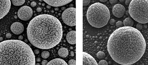 |
| In-depth look: An image of gold atoms on tin from a state-of-the-art scanning electron microscope (left) has relatively poor depth of field�only parts of the image are in sharp focus. By contrast, the entire image from a helium ion microscope image (right) is sharp and clear. NIST researchers are studying helium ion microscopes to improve measurements at the nanoscale that are important to the semiconductor and nanomanufacturing industries.
Credit: NIST |
Abstract:
Just as test pilots push planes to explore their limits, researchers at the National Institute of Standards and Technology (NIST) are probing the newest microscope technology to further improve measurement accuracy at the nanoscale. Better nanoscale measurements are critical for setting standards and improving production in the semiconductor and nanomanufacturing industries.
NIST Studies How New Helium Ion Microscope Measures Up
GAITHERSBURG, MD | Posted on September 3rd, 2008This new microscope technology uses helium ions to generate the signal used to image extremely small objects, a technique analogous to the scanning electron microscope, which was first introduced commercially in the 1960s. Paradoxically, although helium ions are far larger than electrons, they can provide higher resolution images with higher contrast. The depth of field is much better with the new technology too, so more of the image is in focus. "It is the physics," explains Andras Vladar, SEM project leader in NIST's Nanoscale-Metrology Group. "Ions have larger mass and shorter wavelength than electrons, so they can be better for imaging." The images, he says, appear almost three-dimensional, revealing details smaller than a nanometer�the distance spanned by only three atoms in the silicon crystal.
NIST is working to understand the imaging mechanisms of this new technology. The clearest advantage of the helium ion microscope is that the images show the actual edge of a sample better than the SEM, which is critical in precision manufacturing. "Meeting critical dimensions by knowing where an edge is in high-tech manufacturing can mean the difference of hundreds of dollars per piece," explains Michael Postek, chief of the NIST Precision Engineering Division and the nanomanufacturing program manager. Semiconductor manufacturers have multi-million dollar scanning electron microscopes all along their production lines to help control their microchip manufacturing processes.
NIST received the first-ever commercial helium ion microscope, called Orion, from Carl Zeiss, Inc., last summer as part of a cooperative research and development agreement (CRADA). Researchers are test-piloting it in NIST's Advanced Measurement Laboratory (AML), one of the most environmentally stable research facilities in the world. Carefully controlled for vibration, humidity and temperature changes, AML labs are optimal sites to test new microscope technology, say the researchers. "What we are learning," explains Postek, "goes directly back to the manufacturers to improve their products, which allows NIST and industry to obtain the most precise measurements possible. We are transferring NIST technology and sharing our research with the semiconductor industry trade organization, SEMATECH."
One such NIST contribution is "fast imaging," a technique Vladar developed to obtain sharper images. A combination of vibrations at the nanoscale and taking images at high resolutions left certain images fuzzy, similar to what happens when taking a picture of a moving baby with a slow shutter speed. Instead of collecting the signal slowly and getting a fuzzy image, the NIST technique collects many images as fast as possible and merges them using a clever algorithm to reduce the fuzziness and result in a much sharper image.
Zeiss has recently replaced the original Orion with the first-ever Orion Plus, which incorporates many of NIST's suggestions in its design, including an improved cooling system for the helium source for improved imaging.
####
About NIST
Founded in 1901, NIST is a non-regulatory federal agency within the U.S. Department of Commerce. NIST's mission is to promote U.S. innovation and industrial competitiveness by advancing measurement science, standards, and technology in ways that enhance economic security and improve our quality of life.
For more information, please click here
Contacts:
Evelyn Brown
(301) 975-5661
Copyright © NIST
If you have a comment, please Contact us.Issuers of news releases, not 7th Wave, Inc. or Nanotechnology Now, are solely responsible for the accuracy of the content.
Bookmark:


| Related News Press |
News and information
![]() Simulating magnetization in a Heisenberg quantum spin chain April 5th, 2024
Simulating magnetization in a Heisenberg quantum spin chain April 5th, 2024
![]() NRL charters Navy�s quantum inertial navigation path to reduce drift April 5th, 2024
NRL charters Navy�s quantum inertial navigation path to reduce drift April 5th, 2024
![]() Discovery points path to flash-like memory for storing qubits: Rice find could hasten development of nonvolatile quantum memory April 5th, 2024
Discovery points path to flash-like memory for storing qubits: Rice find could hasten development of nonvolatile quantum memory April 5th, 2024
Imaging
![]() Nanoscale CL thermometry with lanthanide-doped heavy-metal oxide in TEM March 8th, 2024
Nanoscale CL thermometry with lanthanide-doped heavy-metal oxide in TEM March 8th, 2024
![]() The USTC realizes In situ electron paramagnetic resonance spectroscopy using single nanodiamond sensors November 3rd, 2023
The USTC realizes In situ electron paramagnetic resonance spectroscopy using single nanodiamond sensors November 3rd, 2023
![]() Observation of left and right at nanoscale with optical force October 6th, 2023
Observation of left and right at nanoscale with optical force October 6th, 2023
Announcements
![]() NRL charters Navy�s quantum inertial navigation path to reduce drift April 5th, 2024
NRL charters Navy�s quantum inertial navigation path to reduce drift April 5th, 2024
![]() Discovery points path to flash-like memory for storing qubits: Rice find could hasten development of nonvolatile quantum memory April 5th, 2024
Discovery points path to flash-like memory for storing qubits: Rice find could hasten development of nonvolatile quantum memory April 5th, 2024
|
|
||
|
|
||
| The latest news from around the world, FREE | ||
|
|
||
|
|
||
| Premium Products | ||
|
|
||
|
Only the news you want to read!
Learn More |
||
|
|
||
|
Full-service, expert consulting
Learn More |
||
|
|
||