Home > Press > New 'nano-positioners' may have atomic-scale precision
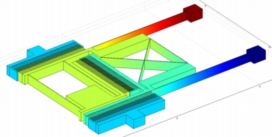 |
| This illustration depicts a tiny device called a monolithic comb drive, which might be used as a high-precision "nanopositioner" for such uses as biological sensors, computer hard drives and other possible applications. The device was created by Jason Vaughn Clark, an assistant professor of electrical and computer engineering and mechanical engineering at Purdue University. (Birck Nanotechnology Center, Purdue University) |
Abstract:
Engineers have created a tiny motorized positioning device that has twice the dexterity of similar devices being developed for applications that include biological sensors and more compact, powerful computer hard drives.
New 'nano-positioners' may have atomic-scale precision
WEST LAFAYETTE, IN | Posted on August 20th, 2008The device, called a monolithic comb drive, might be used as a "nanoscale manipulator" that precisely moves or senses movement and forces. The devices also can be used in watery environments for probing biological molecules, said Jason Vaughn Clark, an assistant professor of electrical and computer engineering and mechanical engineering, who created the design.
The monolithic comb drives could make it possible to improve a class of probe-based sensors that detect viruses and biological molecules. The sensors detect objects using two different components: A probe is moved while at the same time the platform holding the specimen is positioned. The new technology would replace both components with a single one - the monolithic comb drive.
The innovation could allow sensors to work faster and at higher resolution and would be small enough to fit on a microchip. The higher resolution might be used to design future computer hard drives capable of high-density data storage and retrieval. Another possible use might be to fabricate or assemble miniature micro and nanoscale machines.
Research findings were detailed in a technical paper presented in July during the University Government Industry Micro/Nano Symposium in Louisville. The work is based at the Birck Nanotechnology Center at Purdue's Discovery Park.
Conventional comb drives have a pair of comblike sections with "interdigitated fingers," meaning they mesh together. These meshing fingers are drawn toward each other when a voltage is applied. The applied voltage causes the fingers on one comb to become positively charged and the fingers on the other comb to become negatively charged, inducing an attraction between the oppositely charged fingers. If the voltage is removed, the spring-loaded comb sections return to their original position.
By comparison, the new monolithic device has a single structure with two perpendicular comb drives.
Clark calls the device monolithic because it contains comb drive components that are not mechanically and electrically separate. Conventional comb drives are structurally "decoupled" to keep opposite charges separated.
"Comb drives represent an advantage over other technologies," Clark said. "In contrast to piezoelectric actuators that typically deflect, or move, a fraction of a micrometer, comb drives can deflect tens to hundreds of micrometers. And unlike conventional comb drives, which only move in one direction, our new device can move in two directions - left to right, forward and backward - an advance that could really open up the door for many applications."
Clark also has invented a way to determine the precise deflection and force of such microdevices while reducing heat-induced vibrations that could interfere with measurements.
Current probe-based biological sensors have a resolution of about 20 nanometers.
"Twenty nanometers is about the size of 200 atoms, so if you are scanning for a particular molecule, it may be hard to find," Clark said. "With our design, the higher atomic-scale resolution should make it easier to find."
Properly using such devices requires engineers to know precisely how much force is being applied to comb drive sensors and how far they are moving. The new design is based on a technology created by Clark called electro micro metrology, which enables engineers to determine the precise displacement and force that's being applied to, or by, a comb drive. The Purdue researcher is able to measure this force by comparing changes in electrical properties such as capacitance or voltage.
Clark used computational methods called nodal analysis and finite element analysis to design, model and simulate the monolithic comb drives.
The research paper describes how the monolithic comb drive works when voltage is applied. The results show independent left-right and forward-backward movement as functions of applied voltage in color-coded graphics.
The findings are an extension of research to create an ultra-precise measuring system for devices having features on the size scale of nanometers, or billionths of a meter. Clark has led research to create devices that "self-calibrate," meaning they are able to precisely measure themselves. Such measuring methods and standards are needed to better understand and exploit nanometer-scale devices.
The size of the entire device is less than one millimeter, or a thousandth of a meter. The smallest feature size is about three micrometers, roughly one-thirtieth as wide as a human hair.
"You can make them smaller, though," Clark said. "This is a proof of concept. The technology I'm developing should allow researchers to practically and efficiently extract dozens of geometric and material properties of their microdevices just by electronically probing changes in capacitance or voltage."
In addition to finite element analysis, Clark used a simulation tool that he developed called Sugar.
"Sugar is fast and allows me to easily try out many design ideas," he said. "After I narrow down to a particular design, I then use finite element analysis for fine-tuning. Finite element analysis is slow, but it is able to model subtle physical phenomena that Sugar doesn't do as well."
Clark's research team is installing Sugar on the nanoHub this summer, making the tool available to other researchers. The nanoHub is operated by the Network for Computational Nanotechnology, funded by the National Science Foundation and housed at Purdue's Birck Nanotechnology Center.
The researchers also are in the process of fabricating the devices at the Birck Nanotechnology Center.
####
For more information, please click here
Contacts:
Writer:
Emil Venere
(765) 494-4709
Sources:
Jason Vaughn Clark
(765) 494-3437
Purdue News Service:
(765) 494-2096
Copyright © Purdue University
If you have a comment, please Contact us.Issuers of news releases, not 7th Wave, Inc. or Nanotechnology Now, are solely responsible for the accuracy of the content.
Bookmark:


| Related News Press |
News and information
![]() Simulating magnetization in a Heisenberg quantum spin chain April 5th, 2024
Simulating magnetization in a Heisenberg quantum spin chain April 5th, 2024
![]() NRL charters Navy�s quantum inertial navigation path to reduce drift April 5th, 2024
NRL charters Navy�s quantum inertial navigation path to reduce drift April 5th, 2024
![]() Discovery points path to flash-like memory for storing qubits: Rice find could hasten development of nonvolatile quantum memory April 5th, 2024
Discovery points path to flash-like memory for storing qubits: Rice find could hasten development of nonvolatile quantum memory April 5th, 2024
Molecular Nanotechnology
![]() Scientists push the boundaries of manipulating light at the submicroscopic level March 3rd, 2023
Scientists push the boundaries of manipulating light at the submicroscopic level March 3rd, 2023
![]() First electric nanomotor made from DNA material: Synthetic rotary motors at the nanoscale perform mechanical work July 22nd, 2022
First electric nanomotor made from DNA material: Synthetic rotary motors at the nanoscale perform mechanical work July 22nd, 2022
![]() Nanotech scientists create world's smallest origami bird March 17th, 2021
Nanotech scientists create world's smallest origami bird March 17th, 2021
Memory Technology
![]() Utilizing palladium for addressing contact issues of buried oxide thin film transistors April 5th, 2024
Utilizing palladium for addressing contact issues of buried oxide thin film transistors April 5th, 2024
![]() Interdisciplinary: Rice team tackles the future of semiconductors Multiferroics could be the key to ultralow-energy computing October 6th, 2023
Interdisciplinary: Rice team tackles the future of semiconductors Multiferroics could be the key to ultralow-energy computing October 6th, 2023
![]() Researchers discover materials exhibiting huge magnetoresistance June 9th, 2023
Researchers discover materials exhibiting huge magnetoresistance June 9th, 2023
Sensors
Discoveries
![]() Chemical reactions can scramble quantum information as well as black holes April 5th, 2024
Chemical reactions can scramble quantum information as well as black holes April 5th, 2024
![]() New micromaterial releases nanoparticles that selectively destroy cancer cells April 5th, 2024
New micromaterial releases nanoparticles that selectively destroy cancer cells April 5th, 2024
![]() Utilizing palladium for addressing contact issues of buried oxide thin film transistors April 5th, 2024
Utilizing palladium for addressing contact issues of buried oxide thin film transistors April 5th, 2024
Announcements
![]() NRL charters Navy�s quantum inertial navigation path to reduce drift April 5th, 2024
NRL charters Navy�s quantum inertial navigation path to reduce drift April 5th, 2024
![]() Discovery points path to flash-like memory for storing qubits: Rice find could hasten development of nonvolatile quantum memory April 5th, 2024
Discovery points path to flash-like memory for storing qubits: Rice find could hasten development of nonvolatile quantum memory April 5th, 2024
|
|
||
|
|
||
| The latest news from around the world, FREE | ||
|
|
||
|
|
||
| Premium Products | ||
|
|
||
|
Only the news you want to read!
Learn More |
||
|
|
||
|
Full-service, expert consulting
Learn More |
||
|
|
||