Home > Press > Hitachi High-Tech Launches the SU8000
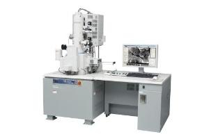 |
| Field Emission Scanning Electron Microscope, SU8000 (Photo: Business Wire) |
Abstract:
A New Type of Scanning Electron Microscope
Hitachi High-Tech Launches the SU8000
Tokyo, Japan | Posted on August 7th, 2008Hitachi High-Technologies Corporation (President: Hidehito Obayashi)(TOKYO:8036) has developed the SU8000, a new type of Field Emission Scanning Electron Microscope (FE-SEM) that features a newly developed top detector. The SU8000 was introduced on August 1.
Hitachi SEMs contribute to research and development in the fields of medicine, biotechnology, and advanced nanotechnology materials. The company's line-up of easy to use SEMs provides these industries with ability to image samples for topographical observations and analyses. The Hitachi SU8000 is now included in the Hitachi line-up of products along with the S-5500, [(Immersion Lens system which generates the highest resolution images in the world(1) (0.4nm at 30kV))], and the S-4800, [(a semi-in-lens type of objective lens to achieve functionality and resolution, on a par with S-5500, but capable of accommodating larger samples (up to 200mm in diameter))].
The new SU8000 features a top detector along with a semi-in-lens type of objective lens. This technology is a further advance on the popular upper backscattered electron detector used in the S-5500. By combining the top detector with the conventional upper detector technology, Hitachi has now developed a new signal detection system for optimum contrast visualization of signals, generated from the sample. These signals include secondary electrons, low-angle backscattered electrons and high-angle backscattered electrons, which are acquired for observation of surface structures.
This top detector can detect high-angle backscattered electrons at low accelerating voltages. This imaging component includes channeling and compositional contrast of the sample's top surface. With Hitachi's beam deceleration technology and the use of the top detector, high-resolution observations can be performed at ultra-low landing voltages. The top detector captures secondary electron signals so the sample's shallow surface information, can be visualized at 100V. The Hitachi SU8000 also includes an upper detector, which provides highly efficient SE signal detection employing Hitachi's proprietary and popular E�B filter technology. This capability provides high-resolution surface structure imaging, while controlling charging. Charge control is provided through a function that enables users to vary the ratio of secondary and backscattered electron signal collection.
The SU8000 features a 24.1-inch widescreen monitor. Compared with the previous 19-inch monitor, the SU8000 monitor improves operability by providing a 1.8-fold increase in pixels and displays the SEM image on a large screen not obscured by the control panel or captured image.
Hitachi High-Technologies is exhibiting the SU8000 at the Microscopy and Microanalysis 2008 to be held in Albuquerque, New Mexico USA from August 3, 2008. The company also plans to introduce the product at the JAIMA Show 2008 (Japan's Exposition of Analytical Instruments and Solutions) to be held at the Makuhari Messe International Convention Complex from September 3, 2008.
Hitachi High-Technologies will begin to ship the product in September 2008 and expects to achieve sales of 200 units per year.
(1) As of July 23, 2008
Standard Features of SU8000
1) The top detector provides compositional and channeling contrast of sample surfaces
2) Improved signal detection capabilities for sample surface observations
3) Charge control function for samples of insulator materials
4) Wide screen LCD monitor
5) Motorized stage as standard
####
About Hitachi High-Technologies Corporation
Hitachi High-Technologies Corporation is a global company that has engaged in a broad range of fields, including device manufacturing equipment, life sciences, information technology, electronic components, and advanced industrial materials. Hitachi High-Technologies is a subsidiary of Hitachi Ltd. Founded in 1947, the Headquarter is located in Tokyo and there are 25 offices in Japan and 63 offices in twenty-nine countries. The company�s consolidated sales is $9.4 in FY2007.
For more information, please click here
Contacts:
Hitachi High Technologies America, Inc.
Hideo Naito
925-218-2800
Semiconductor Equipment Division
or
Hitachi High-Technologies Corporation
Product Marketing Dept.,
Advanced Equipment & Systems Sales Div.,
Semiconductor Equipment Business Group
Tel: +81-3-3504-7714
Public & Investor Relations Group
Tel: +81-3-3504-5637
Copyright © Business Wire 2008
If you have a comment, please Contact us.Issuers of news releases, not 7th Wave, Inc. or Nanotechnology Now, are solely responsible for the accuracy of the content.
Bookmark:


| Related News Press |
News and information
![]() Simulating magnetization in a Heisenberg quantum spin chain April 5th, 2024
Simulating magnetization in a Heisenberg quantum spin chain April 5th, 2024
![]() NRL charters Navy�s quantum inertial navigation path to reduce drift April 5th, 2024
NRL charters Navy�s quantum inertial navigation path to reduce drift April 5th, 2024
![]() Discovery points path to flash-like memory for storing qubits: Rice find could hasten development of nonvolatile quantum memory April 5th, 2024
Discovery points path to flash-like memory for storing qubits: Rice find could hasten development of nonvolatile quantum memory April 5th, 2024
Imaging
![]() Nanoscale CL thermometry with lanthanide-doped heavy-metal oxide in TEM March 8th, 2024
Nanoscale CL thermometry with lanthanide-doped heavy-metal oxide in TEM March 8th, 2024
![]() The USTC realizes In situ electron paramagnetic resonance spectroscopy using single nanodiamond sensors November 3rd, 2023
The USTC realizes In situ electron paramagnetic resonance spectroscopy using single nanodiamond sensors November 3rd, 2023
![]() Observation of left and right at nanoscale with optical force October 6th, 2023
Observation of left and right at nanoscale with optical force October 6th, 2023
Announcements
![]() NRL charters Navy�s quantum inertial navigation path to reduce drift April 5th, 2024
NRL charters Navy�s quantum inertial navigation path to reduce drift April 5th, 2024
![]() Discovery points path to flash-like memory for storing qubits: Rice find could hasten development of nonvolatile quantum memory April 5th, 2024
Discovery points path to flash-like memory for storing qubits: Rice find could hasten development of nonvolatile quantum memory April 5th, 2024
Tools
![]() Ferroelectrically modulate the Fermi level of graphene oxide to enhance SERS response November 3rd, 2023
Ferroelectrically modulate the Fermi level of graphene oxide to enhance SERS response November 3rd, 2023
![]() The USTC realizes In situ electron paramagnetic resonance spectroscopy using single nanodiamond sensors November 3rd, 2023
The USTC realizes In situ electron paramagnetic resonance spectroscopy using single nanodiamond sensors November 3rd, 2023
|
|
||
|
|
||
| The latest news from around the world, FREE | ||
|
|
||
|
|
||
| Premium Products | ||
|
|
||
|
Only the news you want to read!
Learn More |
||
|
|
||
|
Full-service, expert consulting
Learn More |
||
|
|
||