Home > Press > Electron microscopy enters the picometer scale: Juelich scientists are pioneers of ultra-high-resolution electron microscopy
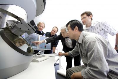 |
| Professor Urban and his staff discuss the atomic structure of an oxide layer of nanoelectronics which is revealed in an electron microscope image. The Ernst Ruska-Centre in Jülich is a joint research platform of excellence operated by Forschungszentrum Juelich and RWTH Aachen University. As a national user center, it provides researchers from science and industry with access to the most powerful electron microscopes currently available. A profound understanding of atomic causes of material properties will provide the basis to tailor materials to specific problems.
Credit: Forschungszentrum Juelich |
Abstract:
Jülich scientists have succeeded in precisely measuring atomic spacings down to a few picometres using new methods in ultrahigh-resolution electron microscopy. This makes it possible to find out decisive parameters determining the physical properties of materials directly on an atomic level in a microscope. Knut Urban from Forschungszentrum Jülich, a member of the Helmholtz Association, reports on this in the latest issue (25 July) of the scientific high-impact journal Science.
Electron microscopy enters the picometer scale: Juelich scientists are pioneers of ultra-high-resolution electron microscopy
Germany | Posted on July 24th, 2008Progress in research in the area of physics is very frequently connected to an increase in the accuracy of measurements, which help researchers to track natural phenomena. With the aid of new methods in electron optics, researchers were able to microscopically measure atomic displacements precisely to a few picometres. A picometre corresponds to a billionth of a millimetre a distance that is one hundred times smaller than the diameter of an atom. This is one of the highlights that Knut Urban, director of the Ernst Ruska-Centre in Jülich, reports on in Science as part of a review of ten years of electron microscopy with aberration-corrected lenses.
Jülich scientists investigated, for example, the configuration of atoms in orthogonal grain boundaries of the oxide superconductor YBa2Cu3O7. These atoms mark the boundary between two areas of the crystalline material with atomic structures that are tilted at an angle of exactly 90° to each other. From microscopic images taken under different conditions, the physicists succeeded in using computers to calculate the quantum-mechanical wave function of the electrons, which served as a basis for determining the exact position of the atoms.
####
About Helmholtz Association of German Research Centres
In doing so, it became apparent that the relatively heavy atomic species barium, copper and yttrium are systematically displaced a few picometres from their ideal position in the grain boundary and that the leighter oxygen atoms follow this displacement. This provides an explanation for the attenuation of superconducting properties, which can be observed when electric current flows over such a grain boundary. This phenomenon is undesired if the superconductor is intended to be used for a loss-free current transport. However, it is useful for the construction of so-called SQUIDs (superconducting quantum interference devices), which exploit the magnetic field dependency of this disturbance to measure smallest magnetic fields, for example, to measure brain waves (magnetoencephalography).
Displacements of a few picometres decide on a whole number of physical properties, which are of eminent importance for technology. Another example is the ferroelectricity of titanates materials. Here, the electrical charges of the individual types of atoms inside the building blocks of crystals, the unit cells, cannot fully compensate for each other as they are not arranged in the necessary symmetry. Therefore, electric dipoles are formed inside the unit cells, which add up over a larger crystal area to form the so-called polarisation. This is used to write information bits. An example is PbZr0.2Ti0.8O3 which is used in chip cards for data storage. With the aid of new electron optical methods, atomic displacements can be measured atom by atom thus making it possible to determine local polarisation for the first time. Knut Urban explains: "This is the beginning of a new physics of materials which enables researchers to determine physical parameters and properties in the nano range through highly precise measurements of the atomic spacings. This will also provide clues on how these properties may be manipulated in order to gain new functions and better functional performance."
Publication:
Studying Atomic Structures by Aberration-Corrected Transmission Electron Microscopy, Knut Urban, Science (25 July 2008)
For more information, please click here
Contacts:
Angela Wenzik
49-246-161-6048
Copyright © Helmholtz Association of German Research Centres
If you have a comment, please Contact us.Issuers of news releases, not 7th Wave, Inc. or Nanotechnology Now, are solely responsible for the accuracy of the content.
Bookmark:


| Related News Press |
Physics
![]() Simulating magnetization in a Heisenberg quantum spin chain April 5th, 2024
Simulating magnetization in a Heisenberg quantum spin chain April 5th, 2024
![]() Chemical reactions can scramble quantum information as well as black holes April 5th, 2024
Chemical reactions can scramble quantum information as well as black holes April 5th, 2024
![]() Nanoscale CL thermometry with lanthanide-doped heavy-metal oxide in TEM March 8th, 2024
Nanoscale CL thermometry with lanthanide-doped heavy-metal oxide in TEM March 8th, 2024
![]() Optically trapped quantum droplets of light can bind together to form macroscopic complexes March 8th, 2024
Optically trapped quantum droplets of light can bind together to form macroscopic complexes March 8th, 2024
|
|
||
|
|
||
| The latest news from around the world, FREE | ||
|
|
||
|
|
||
| Premium Products | ||
|
|
||
|
Only the news you want to read!
Learn More |
||
|
|
||
|
Full-service, expert consulting
Learn More |
||
|
|
||