Home > Press > Applied Materials Launches Breakthrough E3 Equipment and Process Control Solution for Boosting Fab Productivity
 |
Abstract:
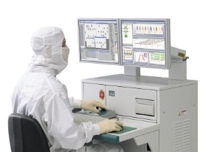
Applied Materials, Inc. today announced its Applied E3™ advanced equipment and process control solution, a comprehensive factory automation (FA) software package for improving the productivity and reducing the costs of semiconductor, flat panel display and photovoltaic solar cell manufacturing. Utilizing proprietary algorithms, the Applied E3 system can boost process capability by >30%, reduce unscheduled down time, and shorten cycle time to achieve up to a 20% increase in overall equipment effectiveness. The Applied E3 system uniquely integrates all critical equipment automation and process control components to deliver the most flexible, user-friendly and powerful fab-wide Equipment Engineering System solution on the market today.
Applied Materials Launches Breakthrough E3 Equipment and Process Control Solution for Boosting Fab Productivity
SANTA CLARA, CA | Posted on July 11th, 2008 "Customers understand that equipment automation is a huge opportunity to exploit the unused potential of their existing assets and to reduce costs," said Manfred Kerschbaum, senior vice president and general manager of Applied Global Services. "The E3 system revolutionizes equipment automation and control technology, which has historically been complex and expensive to implement and maintain. With its graphical development environment and pre-configured modules, the Applied E3 system is quick to deploy and easy to update and extend, offering a fast and cost-effective route to raise factory output. The Applied E3 system has been enthusiastically received by multiple major manufacturers and is currently being used in volume production."
Using an advanced, scalable software architecture, the Applied E3 solution provides a powerful combination of modules. Equipment automation, data collection and logic handling simplify the construction, deployment, and maintenance of automated process control (APC) applications. Fault detection and classification (FDC) collects and analyzes equipment parameters to provide rapid feedback on process performance issues and avoid unexpected failures that decrease productivity. Run-to-run control (R2R) uses patented feedback algorithms to reduce process variability by adjusting processing parameters in real time, enabling more consistent output, higher yield and greater productivity. Equipment performance tracking (EPT) monitors every processing tool in the factory and provides visual and statistical reporting tools to identify bottlenecks and improve factory performance.
The Applied E3 system is part of a broad portfolio of manufacturing automation solutions and services designed to help companies improve their factories' productivity and reduce costs by managing, controlling and automating all aspects of their factory and tool operations. As a leading supplier of capital equipment and processing technology, Applied has effectively utilized its unique experience in equipment design, process control and automation to improve predictability, reduce waste and maximize overall equipment effectiveness.
####
About Applied Materials, Inc.
Applied Materials, Inc. (Nasdaq:AMAT) is the global leader in Nanomanufacturing Technology™ solutions with a broad portfolio of innovative equipment, service and software products for the fabrication of semiconductor chips, flat panel displays, solar photovoltaic cells, flexible electronics and energy efficient glass. At Applied Materials, we apply Nanomanufacturing Technology to improve the way people live.
For more information, please click here
Contacts:
Applied Materials, Inc.
Betty Newboe
408-563-0647 (editorial/media)
Linda Heller
408-986-7977 (financial community)
Copyright © Business Wire 2008
If you have a comment, please Contact us.Issuers of news releases, not 7th Wave, Inc. or Nanotechnology Now, are solely responsible for the accuracy of the content.
Bookmark:


| Related News Press |
News and information
![]() Simulating magnetization in a Heisenberg quantum spin chain April 5th, 2024
Simulating magnetization in a Heisenberg quantum spin chain April 5th, 2024
![]() NRL charters Navy’s quantum inertial navigation path to reduce drift April 5th, 2024
NRL charters Navy’s quantum inertial navigation path to reduce drift April 5th, 2024
![]() Discovery points path to flash-like memory for storing qubits: Rice find could hasten development of nonvolatile quantum memory April 5th, 2024
Discovery points path to flash-like memory for storing qubits: Rice find could hasten development of nonvolatile quantum memory April 5th, 2024
Chip Technology
![]() Discovery points path to flash-like memory for storing qubits: Rice find could hasten development of nonvolatile quantum memory April 5th, 2024
Discovery points path to flash-like memory for storing qubits: Rice find could hasten development of nonvolatile quantum memory April 5th, 2024
![]() Utilizing palladium for addressing contact issues of buried oxide thin film transistors April 5th, 2024
Utilizing palladium for addressing contact issues of buried oxide thin film transistors April 5th, 2024
![]() HKUST researchers develop new integration technique for efficient coupling of III-V and silicon February 16th, 2024
HKUST researchers develop new integration technique for efficient coupling of III-V and silicon February 16th, 2024
Announcements
![]() NRL charters Navy’s quantum inertial navigation path to reduce drift April 5th, 2024
NRL charters Navy’s quantum inertial navigation path to reduce drift April 5th, 2024
![]() Discovery points path to flash-like memory for storing qubits: Rice find could hasten development of nonvolatile quantum memory April 5th, 2024
Discovery points path to flash-like memory for storing qubits: Rice find could hasten development of nonvolatile quantum memory April 5th, 2024
Tools
![]() Ferroelectrically modulate the Fermi level of graphene oxide to enhance SERS response November 3rd, 2023
Ferroelectrically modulate the Fermi level of graphene oxide to enhance SERS response November 3rd, 2023
![]() The USTC realizes In situ electron paramagnetic resonance spectroscopy using single nanodiamond sensors November 3rd, 2023
The USTC realizes In situ electron paramagnetic resonance spectroscopy using single nanodiamond sensors November 3rd, 2023
|
|
||
|
|
||
| The latest news from around the world, FREE | ||
|
|
||
|
|
||
| Premium Products | ||
|
|
||
|
Only the news you want to read!
Learn More |
||
|
|
||
|
Full-service, expert consulting
Learn More |
||
|
|
||