Home > Press > MIT reports finer lines for microchips
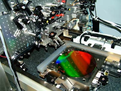 |
| Photo / Ralf Heilmann MIT nanoruler lithography tool with a 300 mm-diameter silicon wafer. |
Abstract:
MIT researchers have achieved a significant advance in nanoscale lithographic technology, used in the manufacture of computer chips and other electronic devices, to make finer patterns of lines over larger areas than have been possible with other methods.
MIT reports finer lines for microchips
Cambridge, MA | Posted on July 10th, 2008Their new technique could pave the way for next-generation computer memory and integrated-circuit chips, as well as advanced solar cells and other devices.
The team has created lines about 25 nanometers (billionths of a meter) wide separated by 25 nm spaces. For comparison, the most advanced commercially available computer chips today have a minimum feature size of 65 nm. Intel recently announced that it will start manufacturing at the 32 nm minimum line-width scale in 2009, and the industry roadmap calls for 25 nm features in the 2013-2015 time frame.
The MIT technique could also be economically attractive because it works without the chemically amplified resists, immersion lithography techniques and expensive lithography tools that are widely considered essential to work at this scale with optical lithography. Periodic patterns at the nanoscale, while having many important scientific and commercial applications, are notoriously difficult to produce with low cost and high yield. The new method could make possible the commercialization of many new nanotechnology inventions that have languished in laboratories due to the lack of a viable manufacturing method.
The MIT team includes Mark Schattenburg and Ralf Heilmann of the MIT Kavli Institute of Astrophysics and Space Research and graduate students Chih-Hao Chang and Yong Zhao of the Department of Mechanical Engineering. Their results have been accepted for publication in the journal Optics Letters and were recently presented at the 52nd International Conference on Electron, Ion and Photon Beam Technology and Nanofabrication in Portland, Ore.
Schattenburg and colleagues used a technique known as interference lithography (IL) to generate the patterns, but they did so using a tool called the nanoruler--built by MIT graduate students--that is designed to perform a particularly high precision variant of IL called scanning-beam interference lithography, or SBIL. This recently developed technique uses 100 MHz sound waves, controlled by custom high-speed electronics, to diffract and frequency-shift the laser light, resulting in rapid patterning of large areas with unprecedented control over feature geometry.
While IL has been around for a long time, the SBIL technique has enabled, for the first time, the precise and repeatable pattern registration and overlay over large areas, thanks to a new high-precision phase detection algorithm developed by Zhao and a novel image reversal process developed by Chang.
According to Schattenburg, "What we're finding is that control of the lithographic imaging process is no longer the limiting step. Material issues such as line sidewall roughness are now a major barrier to still-finer length scales. However, there are several new technologies on the horizon that have the potential for alleviating these problems. These results demonstrate that there's still a lot of room left for scale shrinkage in optical lithography. We don't see any insurmountable roadblocks just yet."
The MIT team performed the research in the Space Nanotechnology Laboratory of the MIT Kavli Institute of Astrophysics and Space Research, with financial support from NASA and NSF.
####
About MIT
The mission of MIT is to advance knowledge and educate students in science, technology, and other areas of scholarship that will best serve the nation and the world in the 21st century.
For more information, please click here
Contacts:
MIT News Office
Phone 617-253-2700
Room 11-400
77 Massachusetts Ave.
Cambridge, MA 02139-4307
Copyright © MIT
If you have a comment, please Contact us.Issuers of news releases, not 7th Wave, Inc. or Nanotechnology Now, are solely responsible for the accuracy of the content.
Bookmark:


| Related News Press |
News and information
![]() Simulating magnetization in a Heisenberg quantum spin chain April 5th, 2024
Simulating magnetization in a Heisenberg quantum spin chain April 5th, 2024
![]() NRL charters Navy�s quantum inertial navigation path to reduce drift April 5th, 2024
NRL charters Navy�s quantum inertial navigation path to reduce drift April 5th, 2024
![]() Discovery points path to flash-like memory for storing qubits: Rice find could hasten development of nonvolatile quantum memory April 5th, 2024
Discovery points path to flash-like memory for storing qubits: Rice find could hasten development of nonvolatile quantum memory April 5th, 2024
Chip Technology
![]() Discovery points path to flash-like memory for storing qubits: Rice find could hasten development of nonvolatile quantum memory April 5th, 2024
Discovery points path to flash-like memory for storing qubits: Rice find could hasten development of nonvolatile quantum memory April 5th, 2024
![]() Utilizing palladium for addressing contact issues of buried oxide thin film transistors April 5th, 2024
Utilizing palladium for addressing contact issues of buried oxide thin film transistors April 5th, 2024
![]() HKUST researchers develop new integration technique for efficient coupling of III-V and silicon February 16th, 2024
HKUST researchers develop new integration technique for efficient coupling of III-V and silicon February 16th, 2024
Nanoelectronics
![]() Interdisciplinary: Rice team tackles the future of semiconductors Multiferroics could be the key to ultralow-energy computing October 6th, 2023
Interdisciplinary: Rice team tackles the future of semiconductors Multiferroics could be the key to ultralow-energy computing October 6th, 2023
![]() Key element for a scalable quantum computer: Physicists from Forschungszentrum J�lich and RWTH Aachen University demonstrate electron transport on a quantum chip September 23rd, 2022
Key element for a scalable quantum computer: Physicists from Forschungszentrum J�lich and RWTH Aachen University demonstrate electron transport on a quantum chip September 23rd, 2022
![]() Reduced power consumption in semiconductor devices September 23rd, 2022
Reduced power consumption in semiconductor devices September 23rd, 2022
![]() Atomic level deposition to extend Moore�s law and beyond July 15th, 2022
Atomic level deposition to extend Moore�s law and beyond July 15th, 2022
Discoveries
![]() Chemical reactions can scramble quantum information as well as black holes April 5th, 2024
Chemical reactions can scramble quantum information as well as black holes April 5th, 2024
![]() New micromaterial releases nanoparticles that selectively destroy cancer cells April 5th, 2024
New micromaterial releases nanoparticles that selectively destroy cancer cells April 5th, 2024
![]() Utilizing palladium for addressing contact issues of buried oxide thin film transistors April 5th, 2024
Utilizing palladium for addressing contact issues of buried oxide thin film transistors April 5th, 2024
Announcements
![]() NRL charters Navy�s quantum inertial navigation path to reduce drift April 5th, 2024
NRL charters Navy�s quantum inertial navigation path to reduce drift April 5th, 2024
![]() Discovery points path to flash-like memory for storing qubits: Rice find could hasten development of nonvolatile quantum memory April 5th, 2024
Discovery points path to flash-like memory for storing qubits: Rice find could hasten development of nonvolatile quantum memory April 5th, 2024
|
|
||
|
|
||
| The latest news from around the world, FREE | ||
|
|
||
|
|
||
| Premium Products | ||
|
|
||
|
Only the news you want to read!
Learn More |
||
|
|
||
|
Full-service, expert consulting
Learn More |
||
|
|
||