Home > Press > FEI Introduces New Category of Extreme High Resolution Scanning Electron Microscopy
 |
Abstract:
New Magellan SEM First to Enable Rapid 3D Surface Imaging at Sub-Nanometer Resolution
FEI Introduces New Category of Extreme High Resolution Scanning Electron Microscopy
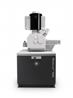
HILLSBORO, OR | Posted on July 7th, 2008With its announcement today of the Magellan� Family, FEI Company (Nasdaq: FEIC) introduced a new class of instruments called extreme high-resolution scanning electron microscopes (XHR SEMs). The Magellan XHR SEM allows scientists and engineers to quickly see things they could not see before, such as 3D surface images at many different angles and at resolutions below one nanometer (about the size of ten hydrogen atoms, side-by-side). Most importantly, the Magellan XHR SEM images samples at very low beam energies, avoiding distortions otherwise caused by the beam penetrating into the material below.
"The Magellan XHR SEM is the most significant electron optics innovation since FEI introduced the Titan� Family three years ago," said Dr. Rob Fastenau, FEI's executive vice president, marketing and technology. "Magellan is in a class by itself, just as Titan is for transmission electron microscopes, and our innovative Helios NanoLab� family is for DualBeam� systems. Magellan is the only family of instruments to make sub-nanometer resolution accessible in a practical sense to non-experts and without restriction on samples�constraints that have previously limited the utility and acceptance of other systems. As the performance benchmark in its category, Magellan is another demonstration of FEI's deep commitment to being the leading innovator of high-performance solutions in all of our markets."
Sub-nanometer resolution has critical value in scientific research and industrial R&D. In addition, it is an absolute requirement in process development, monitoring and control applications in advanced semiconductor manufacturing. The Magellan Family extends this capability to applications that were previously impossible or impractical with conventional SEM, transmission electron microscope (TEM) or focused ion beam (FIB) systems.
For example, the ability to provide sub-nanometer resolution over a broad range of beam energies, from less than one kilovolt (kV) to 30kV, allows semiconductor manufacturers to see critical detail on complex three-dimensional structures in 32nm nodes and below, with unprecedented clarity and contrast. Researchers in materials science will now have the ability to generate high-resolution, surface-sensitive images of carbon nanotubes, nanowires and catalysts without the image distortions caused by electrical charging from higher energy electron beams. Across the board, the Magellan Family extends the range of nanoscale imaging and analysis, with the speed and ease-of-use of traditional SEMs.
The Magellan Family's performance derives from the integration of new electron optical elements, proprietary electron gun technology, a highly accurate five-axis piezo-ceramic stage and high stability platform with fully configurable analytical chamber. The stage readily accommodates large samples or multiple smaller samples, while providing fast, accurate navigation and unequaled stability.
The Magellan Family comes in two models: The Magellan 400 is optimized for scientific research while the Magellan 400L is optimized for semiconductor labs. The semiconductor lab model comes with a load-lock feature that speeds-up sample throughput, and includes a retractable solid state backscatter electron detector (SSBSED) and S2 compliance kit. Both models have an optional, full environmental enclosure to isolate the instrument from thermal and acoustic interferences, ensuring peak performance while relaxing site requirements and facility preparation costs. The Magellan Family is available for purchase now, with initial shipments planned to begin in September 2008.
####
About FEI Company
FEI (Nasdaq: FEIC) is the world leader in pioneering technologies and applications that deliver imaging solutions for 3D characterization, analysis and modification/prototyping with resolutions down to the sub-�ngstr�m level. Our customers, working in advanced research and manufacturing, are supported by field-experienced applications specialists. They have open access to FEI�s prestigious global user network so they can succeed in accelerating nanoscale discovery and contribute to better living through new product commercialization. FEI�s NanoPorts in North America, Europe and Asia provide centers of technical excellence where our world-class community of customers and specialists collaborate on the ongoing development of new ideas and innovative solutions. FEI has sales and service operations in more than 50 countries around the world.
FEI Safe Harbor Statement
This news release contains forward-looking statements that include statements about future performance and new applications of our Magellan Family of XHR SEMs. Factors that could affect these forward-looking statements include but are not limited to the inability of customers to develop and deploy the expected new applications. Additional factors that could affect these forward-looking statements include, but are not limited to unforeseen problems or technology challenges arising in the beta phase of the product introduction; problems moving the product from beta to production release; problems in manufacturing the product; and failure of a key supplier or technology partner. Please also refer to our Form 10-K, Forms 10-Q, Forms 8-K and other filings with the U.S. Securities and Exchange Commission for additional information on these factors and other factors that could cause actual results to differ materially from the forward-looking statements. FEI assumes no duty to update forward-looking statements.
The FEI logo, Magellan, Titan, NanoLab and DualBeam are trademarks of FEI Company.
For more information, please click here
Contacts:
Media Contact:
Sandy Fewkes, Principal
MindWrite Communications, Inc
+1 408 224 4024
FEI Company
Fletcher Chamberlin (investors and analysts)
Investor Relations
+1 503 726 7710
Copyright © FEI Company
If you have a comment, please Contact us.Issuers of news releases, not 7th Wave, Inc. or Nanotechnology Now, are solely responsible for the accuracy of the content.
Bookmark:


| Related News Press |
News and information
![]() Simulating magnetization in a Heisenberg quantum spin chain April 5th, 2024
Simulating magnetization in a Heisenberg quantum spin chain April 5th, 2024
![]() NRL charters Navy�s quantum inertial navigation path to reduce drift April 5th, 2024
NRL charters Navy�s quantum inertial navigation path to reduce drift April 5th, 2024
![]() Discovery points path to flash-like memory for storing qubits: Rice find could hasten development of nonvolatile quantum memory April 5th, 2024
Discovery points path to flash-like memory for storing qubits: Rice find could hasten development of nonvolatile quantum memory April 5th, 2024
Imaging
![]() Nanoscale CL thermometry with lanthanide-doped heavy-metal oxide in TEM March 8th, 2024
Nanoscale CL thermometry with lanthanide-doped heavy-metal oxide in TEM March 8th, 2024
![]() The USTC realizes In situ electron paramagnetic resonance spectroscopy using single nanodiamond sensors November 3rd, 2023
The USTC realizes In situ electron paramagnetic resonance spectroscopy using single nanodiamond sensors November 3rd, 2023
![]() Observation of left and right at nanoscale with optical force October 6th, 2023
Observation of left and right at nanoscale with optical force October 6th, 2023
Announcements
![]() NRL charters Navy�s quantum inertial navigation path to reduce drift April 5th, 2024
NRL charters Navy�s quantum inertial navigation path to reduce drift April 5th, 2024
![]() Discovery points path to flash-like memory for storing qubits: Rice find could hasten development of nonvolatile quantum memory April 5th, 2024
Discovery points path to flash-like memory for storing qubits: Rice find could hasten development of nonvolatile quantum memory April 5th, 2024
Tools
![]() Ferroelectrically modulate the Fermi level of graphene oxide to enhance SERS response November 3rd, 2023
Ferroelectrically modulate the Fermi level of graphene oxide to enhance SERS response November 3rd, 2023
![]() The USTC realizes In situ electron paramagnetic resonance spectroscopy using single nanodiamond sensors November 3rd, 2023
The USTC realizes In situ electron paramagnetic resonance spectroscopy using single nanodiamond sensors November 3rd, 2023
|
|
||
|
|
||
| The latest news from around the world, FREE | ||
|
|
||
|
|
||
| Premium Products | ||
|
|
||
|
Only the news you want to read!
Learn More |
||
|
|
||
|
Full-service, expert consulting
Learn More |
||
|
|
||