Home > Press > New Process Creates 3-D Nanostructures with Magnetic Materials
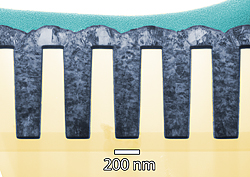 |
| Working in the trenches: Transmission electron microscopy image of a thin cross section of 160 nanometer trenches shows deposited nickel completely filling the features without voids. (Color added for clarity.)
Credit: NIST |
Abstract:
Materials scientists at the National Institute of Standards and Technology (NIST) have developed a process to build complex, three-dimensional nanoscale structures of magnetic materials such as nickel or nickel-iron alloys using techniques compatible with standard semiconductor manufacturing. The process, described in a recent paper,* could enable whole new classes of sensors and microelectromechanical (MEMS) devices.
New Process Creates 3-D Nanostructures with Magnetic Materials
GAITHERSBURG, MD | Posted on June 26th, 2008The NIST team also demonstrated that key process variables are linked to relatively quick and inexpensive electrochemical measurements, pointing the way to a fast and efficient way to optimize the process for new materials.
The NIST process is a variation of a technique called "Damascene metallization" that often is used to create complicated three-dimensional copper interconnections, the "wiring" that links circuit elements across multiple layers in advanced, large-scale integrated circuits. Named after the ancient art of creating designs with metal-in-metal inlays, the process involves etching complex patterns of horizontal trenches and vertical "vias" in the surface of the wafer and then uses an electroplating process to fill them with copper. The high aspect ratio features may range from tens of nanometers to hundreds of microns in width. Once filled, the surface of the disk is ground and polished down to remove the excess copper, leaving behind the trench and via pattern.
The big trick in Damascene metallization is ensuring that the deposited metal completely fills in the deep, narrow trenches without leaving voids. This can be done by adding a chemical to the electrodeposition solution to prevent the metal from building up too quickly on the sides of the trenches and by careful control of the deposition process, but both the chemistry and the process variables turn out to be significantly different for active ferromagnetic materials than for passive materials like copper. In addition to devising a working combination of electrolytes and additives to do Damascene metallization with nickel and a nickel-iron alloy, the NIST team demonstrated straightforward measurements for identifying and optimizing the feature-filling process thereby providing an efficient path for the creation of quality nanoscale ferromagnet structures.
The new process makes it feasible to create complex three-dimensional MEMS devices such as inductors and actuators that combine magnetic alloys with non-magnetic metallizations such as copper interconnects using existing production systems.
* C.H. Lee, J.E. Bonevich, J.E. Davies and T.P. Moffat. Magnetic materials for three-dimensional Damascene metallization: void-free electrodeposition of Ni and Ni70Fe30 using 2-mercapto-5-benzimidazolesulfonic acid. Journal of The Electrochemical Society, 155 (7) D499-D507 (2008).
####
About NIST
Founded in 1901, NIST is a non-regulatory federal agency within the U.S. Department of Commerce. NIST's mission is to promote U.S. innovation and industrial competitiveness by advancing measurement science, standards, and technology in ways that enhance economic security and improve our quality of life.
For more information, please click here
Contacts:
Michael Baum
(301) 975-2763
Copyright © NIST
If you have a comment, please Contact us.Issuers of news releases, not 7th Wave, Inc. or Nanotechnology Now, are solely responsible for the accuracy of the content.
Bookmark:


| Related News Press |
News and information
![]() Simulating magnetization in a Heisenberg quantum spin chain April 5th, 2024
Simulating magnetization in a Heisenberg quantum spin chain April 5th, 2024
![]() NRL charters Navy�s quantum inertial navigation path to reduce drift April 5th, 2024
NRL charters Navy�s quantum inertial navigation path to reduce drift April 5th, 2024
![]() Discovery points path to flash-like memory for storing qubits: Rice find could hasten development of nonvolatile quantum memory April 5th, 2024
Discovery points path to flash-like memory for storing qubits: Rice find could hasten development of nonvolatile quantum memory April 5th, 2024
MEMS
Discoveries
![]() Chemical reactions can scramble quantum information as well as black holes April 5th, 2024
Chemical reactions can scramble quantum information as well as black holes April 5th, 2024
![]() New micromaterial releases nanoparticles that selectively destroy cancer cells April 5th, 2024
New micromaterial releases nanoparticles that selectively destroy cancer cells April 5th, 2024
![]() Utilizing palladium for addressing contact issues of buried oxide thin film transistors April 5th, 2024
Utilizing palladium for addressing contact issues of buried oxide thin film transistors April 5th, 2024
Materials/Metamaterials/Magnetoresistance
![]() Nanoscale CL thermometry with lanthanide-doped heavy-metal oxide in TEM March 8th, 2024
Nanoscale CL thermometry with lanthanide-doped heavy-metal oxide in TEM March 8th, 2024
![]() Focused ion beam technology: A single tool for a wide range of applications January 12th, 2024
Focused ion beam technology: A single tool for a wide range of applications January 12th, 2024
Announcements
![]() NRL charters Navy�s quantum inertial navigation path to reduce drift April 5th, 2024
NRL charters Navy�s quantum inertial navigation path to reduce drift April 5th, 2024
![]() Discovery points path to flash-like memory for storing qubits: Rice find could hasten development of nonvolatile quantum memory April 5th, 2024
Discovery points path to flash-like memory for storing qubits: Rice find could hasten development of nonvolatile quantum memory April 5th, 2024
|
|
||
|
|
||
| The latest news from around the world, FREE | ||
|
|
||
|
|
||
| Premium Products | ||
|
|
||
|
Only the news you want to read!
Learn More |
||
|
|
||
|
Full-service, expert consulting
Learn More |
||
|
|
||