Home > Press > IP Profile: Nanoswitches based on Crystalline Conductive Polymer Nanoneedles
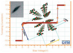 |
| Switching behavior of the nanoneedle vs. gold |
Abstract:
As the density of electronic circuits increases, electronic researchers are looking to nano-scale devices. Typical organic nanoswitches are slow (~ minutes) and are difficult to produce. Our conductive polymer nanocrystal system has switching times on the order of milliseconds and is scalable. This invention will allow for use of this nanoswitch system in conventional commercial micro or nanocircuits.
IP Profile: Nanoswitches based on Crystalline Conductive Polymer Nanoneedles
Boston, MA | Posted on May 22nd, 2008Organization: Center for Engineered Polymeric Materials (CEPM), A NYSTAR sponsored CART center, College of Staten Island
Primary Market: Electronics
Technology Contact: Dr. Nan Loh Yang, Director of CEPM
IP profile courtesy of Nan Loh Yang, Director of Center for Engineered Polymeric Materials (CEPM), College of Staten Island
Professor Nan-Loh Yang, Director of the NYSTAR designated Center for Engineered Polymeric Materials (CEPM) indicated that these conductive polymer nanoswitches are especially suited for use in nanoelectronics and nanocircuitry and have switching speeds that are several orders of magnitude faster than typical organic switching materials. This crystalline conductive polymer material can cycle between two states based on an applied threshold bias voltage (~3V). This switching phenomenon has potential applications in circuit switching elements, e.g. driving organic electroluminescent (EL) display panels or for high-density memories.
Methods of manufacturing the nanoparticle polymer structure in the nanoswitch are based on a novel interfacial oxidative polymerization technique. Conductive polymers such as polythiophenes, polypyrroles and polyaniline were employed but were not limited to these polymer families. These highly crystalline conductive polymers have very rapid switching times which allows for the use of these materials in the targeted applications. The use of these electronics materials can open the door to many applications in both current and future circuit designs. CEPM is seeking partners in joint development of this invention. The immediate aim would be to make developmental prototype nanoswitches that could be used in current commercial devices.
####
About NSTI
The Nano Science and Technology Institute (NSTI) is chartered with the promotion and integration of nano and other advanced technologies through education, technology and business development. NSTI accomplishes this mission through its offerings of continuing education programs, scientific and business publishing and community outreach. NSTI produces the annual Nanotech conference and trade show, the most comprehensive international nanotechnology convention in the world. NSTI also produces the semi-annual Nanotech Venture, Nanotech Industrial Impact Workshop, Nano Impact Summit and the Nanotech Course Series in the US and Europe. NSTI was founded in 1997 as a result of the merger between various scientific societies, and is headquartered in Cambridge, Massachusetts with additional offices in California and Switzerland.
For more information, please click here
Contacts:
Sarah Wenning
696 San Ramon Valley Blvd., Ste. 423
Danville, CA 94526
Ph: (925) 901-4959
Fax: (925) 886-8461
Copyright © NSTI
If you have a comment, please Contact us.Issuers of news releases, not 7th Wave, Inc. or Nanotechnology Now, are solely responsible for the accuracy of the content.
Bookmark:


| Related News Press |
News and information
![]() Simulating magnetization in a Heisenberg quantum spin chain April 5th, 2024
Simulating magnetization in a Heisenberg quantum spin chain April 5th, 2024
![]() NRL charters Navy�s quantum inertial navigation path to reduce drift April 5th, 2024
NRL charters Navy�s quantum inertial navigation path to reduce drift April 5th, 2024
![]() Discovery points path to flash-like memory for storing qubits: Rice find could hasten development of nonvolatile quantum memory April 5th, 2024
Discovery points path to flash-like memory for storing qubits: Rice find could hasten development of nonvolatile quantum memory April 5th, 2024
Nanoelectronics
![]() Interdisciplinary: Rice team tackles the future of semiconductors Multiferroics could be the key to ultralow-energy computing October 6th, 2023
Interdisciplinary: Rice team tackles the future of semiconductors Multiferroics could be the key to ultralow-energy computing October 6th, 2023
![]() Key element for a scalable quantum computer: Physicists from Forschungszentrum J�lich and RWTH Aachen University demonstrate electron transport on a quantum chip September 23rd, 2022
Key element for a scalable quantum computer: Physicists from Forschungszentrum J�lich and RWTH Aachen University demonstrate electron transport on a quantum chip September 23rd, 2022
![]() Reduced power consumption in semiconductor devices September 23rd, 2022
Reduced power consumption in semiconductor devices September 23rd, 2022
![]() Atomic level deposition to extend Moore�s law and beyond July 15th, 2022
Atomic level deposition to extend Moore�s law and beyond July 15th, 2022
Announcements
![]() NRL charters Navy�s quantum inertial navigation path to reduce drift April 5th, 2024
NRL charters Navy�s quantum inertial navigation path to reduce drift April 5th, 2024
![]() Discovery points path to flash-like memory for storing qubits: Rice find could hasten development of nonvolatile quantum memory April 5th, 2024
Discovery points path to flash-like memory for storing qubits: Rice find could hasten development of nonvolatile quantum memory April 5th, 2024
Patents/IP/Tech Transfer/Licensing
![]() Getting drugs across the blood-brain barrier using nanoparticles March 3rd, 2023
Getting drugs across the blood-brain barrier using nanoparticles March 3rd, 2023
![]() Metasurfaces control polarized light at will: New research unlocks the hidden potential of metasurfaces August 13th, 2021
Metasurfaces control polarized light at will: New research unlocks the hidden potential of metasurfaces August 13th, 2021
![]() Arrowhead Pharmaceuticals Announces Closing of Agreement with Takeda November 27th, 2020
Arrowhead Pharmaceuticals Announces Closing of Agreement with Takeda November 27th, 2020
Events/Classes
![]() Researchers demonstrate co-propagation of quantum and classical signals: Study shows that quantum encryption can be implemented in existing fiber networks January 20th, 2023
Researchers demonstrate co-propagation of quantum and classical signals: Study shows that quantum encryption can be implemented in existing fiber networks January 20th, 2023
|
|
||
|
|
||
| The latest news from around the world, FREE | ||
|
|
||
|
|
||
| Premium Products | ||
|
|
||
|
Only the news you want to read!
Learn More |
||
|
|
||
|
Full-service, expert consulting
Learn More |
||
|
|
||