Home > Press > R&D Profile: Nanotechnology, Contribution of Fraunhofer IZM, Department SIIT: R. Aschenbrenner, Fraunhofer
 |
| Packaging Technologies for nano electronics |
Abstract:
The basis for the use of nanotechnologies in microelectronic packaging is the synergetic connection of the typical nano-disciplines physics and chemistry with biology and different engineering sciences in order to develop production technologies, which are suitable for nano integration.
R&D Profile: Nanotechnology, Contribution of Fraunhofer IZM, Department SIIT: R. Aschenbrenner, Fraunhofer
Boston, MA | Posted on May 22nd, 2008R&D Overview Provided By Rolf Aschenbrenner, Head of Chip Interconnection Technologies Department, Fraunhofer Institute for Reliability and Microintegration Berlin (IZM).
Dr. Aschenmbrennar is a featured speaker at next month's NSTI Nanotech conference.
The main topics for the so-called nano packaging are the integration of digital electronics, photonics, high frequency ICs and biological functionality into a monolithic system and the realization of solutions for contacting of nano-scale structures. These topics are embedded into an infrastructure, which includes the handling and processing of components, materials and adapted analytics:
* "Nano Materials", e. g. nano particles, nano composites und nano-structured surfaces
* "Nano Processes", e. g. self assembly of 2- and 3D structures, handling and dispersing of nano particles, contacting at low temperatures by bonding of nano-structured surfaces
* "Nano Tools", e. g. analytics, modelling and simulation of nano materials and processes
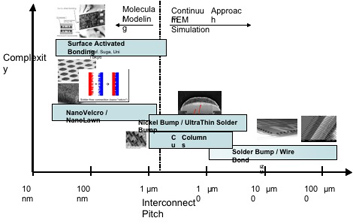
When focusing on production technologies, the main research emphasizes are the development of lower-cost nano assembly processes suitable for mass production and the necessary tools for process controlling and the evaluation of the reliability. Examples for the use of nano technology are shown in picture 1 with a presentation of possible packaging technologies for nano-optimized contacting, in picture 2 with the use of CNTs for the optimization of miniaturization contacts and in picture 3 with the use of nano-scale filling materials for the increase of the filling degree for the optimization of the extension coefficient or rather by adding of bentonites for the improvement of the moisture barrier characteristics in an encapsulation material.
####
About NSTI
The Nano Science and Technology Institute (NSTI) is chartered with the promotion and integration of nano and other advanced technologies through education, technology and business development. NSTI accomplishes this mission through its offerings of continuing education programs, scientific and business publishing and community outreach. NSTI produces the annual Nanotech conference and trade show, the most comprehensive international nanotechnology convention in the world. NSTI also produces the semi-annual Nanotech Venture, Nanotech Industrial Impact Workshop, Nano Impact Summit and the Nanotech Course Series in the US and Europe. NSTI was founded in 1997 as a result of the merger between various scientific societies, and is headquartered in Cambridge, Massachusetts with additional offices in California and Switzerland.
For more information, please click here
Contacts:
Sarah Wenning
696 San Ramon Valley Blvd., Ste. 423
Danville, CA 94526
Ph: (925) 901-4959
Fax: (925) 886-8461
Copyright © NSTI
If you have a comment, please Contact us.Issuers of news releases, not 7th Wave, Inc. or Nanotechnology Now, are solely responsible for the accuracy of the content.
Bookmark:


| Related News Press |
Physics
![]() Simulating magnetization in a Heisenberg quantum spin chain April 5th, 2024
Simulating magnetization in a Heisenberg quantum spin chain April 5th, 2024
![]() Nanoscale CL thermometry with lanthanide-doped heavy-metal oxide in TEM March 8th, 2024
Nanoscale CL thermometry with lanthanide-doped heavy-metal oxide in TEM March 8th, 2024
News and information
![]() Simulating magnetization in a Heisenberg quantum spin chain April 5th, 2024
Simulating magnetization in a Heisenberg quantum spin chain April 5th, 2024
![]() NRL charters Navy�s quantum inertial navigation path to reduce drift April 5th, 2024
NRL charters Navy�s quantum inertial navigation path to reduce drift April 5th, 2024
![]() Discovery points path to flash-like memory for storing qubits: Rice find could hasten development of nonvolatile quantum memory April 5th, 2024
Discovery points path to flash-like memory for storing qubits: Rice find could hasten development of nonvolatile quantum memory April 5th, 2024
Chemistry
![]() What heat can tell us about battery chemistry: using the Peltier effect to study lithium-ion cells March 8th, 2024
What heat can tell us about battery chemistry: using the Peltier effect to study lithium-ion cells March 8th, 2024
![]() Nanoscale CL thermometry with lanthanide-doped heavy-metal oxide in TEM March 8th, 2024
Nanoscale CL thermometry with lanthanide-doped heavy-metal oxide in TEM March 8th, 2024
Nanoelectronics
![]() Interdisciplinary: Rice team tackles the future of semiconductors Multiferroics could be the key to ultralow-energy computing October 6th, 2023
Interdisciplinary: Rice team tackles the future of semiconductors Multiferroics could be the key to ultralow-energy computing October 6th, 2023
![]() Key element for a scalable quantum computer: Physicists from Forschungszentrum J�lich and RWTH Aachen University demonstrate electron transport on a quantum chip September 23rd, 2022
Key element for a scalable quantum computer: Physicists from Forschungszentrum J�lich and RWTH Aachen University demonstrate electron transport on a quantum chip September 23rd, 2022
![]() Reduced power consumption in semiconductor devices September 23rd, 2022
Reduced power consumption in semiconductor devices September 23rd, 2022
![]() Atomic level deposition to extend Moore�s law and beyond July 15th, 2022
Atomic level deposition to extend Moore�s law and beyond July 15th, 2022
Announcements
![]() NRL charters Navy�s quantum inertial navigation path to reduce drift April 5th, 2024
NRL charters Navy�s quantum inertial navigation path to reduce drift April 5th, 2024
![]() Discovery points path to flash-like memory for storing qubits: Rice find could hasten development of nonvolatile quantum memory April 5th, 2024
Discovery points path to flash-like memory for storing qubits: Rice find could hasten development of nonvolatile quantum memory April 5th, 2024
Events/Classes
![]() Researchers demonstrate co-propagation of quantum and classical signals: Study shows that quantum encryption can be implemented in existing fiber networks January 20th, 2023
Researchers demonstrate co-propagation of quantum and classical signals: Study shows that quantum encryption can be implemented in existing fiber networks January 20th, 2023
Nanobiotechnology
![]() New micromaterial releases nanoparticles that selectively destroy cancer cells April 5th, 2024
New micromaterial releases nanoparticles that selectively destroy cancer cells April 5th, 2024
![]() Good as gold - improving infectious disease testing with gold nanoparticles April 5th, 2024
Good as gold - improving infectious disease testing with gold nanoparticles April 5th, 2024
![]() Researchers develop artificial building blocks of life March 8th, 2024
Researchers develop artificial building blocks of life March 8th, 2024
Photonics/Optics/Lasers
![]() With VECSELs towards the quantum internet Fraunhofer: IAF achieves record output power with VECSEL for quantum frequency converters April 5th, 2024
With VECSELs towards the quantum internet Fraunhofer: IAF achieves record output power with VECSEL for quantum frequency converters April 5th, 2024
![]() Nanoscale CL thermometry with lanthanide-doped heavy-metal oxide in TEM March 8th, 2024
Nanoscale CL thermometry with lanthanide-doped heavy-metal oxide in TEM March 8th, 2024
![]() Optically trapped quantum droplets of light can bind together to form macroscopic complexes March 8th, 2024
Optically trapped quantum droplets of light can bind together to form macroscopic complexes March 8th, 2024
![]() HKUST researchers develop new integration technique for efficient coupling of III-V and silicon February 16th, 2024
HKUST researchers develop new integration technique for efficient coupling of III-V and silicon February 16th, 2024
|
|
||
|
|
||
| The latest news from around the world, FREE | ||
|
|
||
|
|
||
| Premium Products | ||
|
|
||
|
Only the news you want to read!
Learn More |
||
|
|
||
|
Full-service, expert consulting
Learn More |
||
|
|
||