Home > Press > Making a Good Impression: Nanoimprint Lithography Tests at NIST
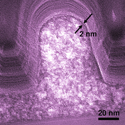 |
| Electron micrograph shows a cross-section of a typical SOG microcircuit feature. Nanoporous regions in the interior are lighter. The process forms a dense, stronger skin about 2 nanometers thick on the outside. (Color added for clarity.)
Credit: NIST |
Abstract:
In what should be good news for integrated circuit manufacturers, recent studies by the National Institute of Standards and Technology (NIST) have helped resolve two important questions about an emerging microcircuit manufacturing technology called nanoimprint lithography—yes, it can accurately stamp delicate insulating structures on advanced microchips, and, no, it doesn't damage them, in fact it makes them better.
Making a Good Impression: Nanoimprint Lithography Tests at NIST
GAITHERSBURG, MD | Posted on April 29th, 2008An emerging manufacturing technique, nanoimprint lithography (NIL) is basically an embossing process. A stamp with a nanoscale pattern in its surface is pressed into a soft film on the surface of a semiconductor wafer. The film is hardened, usually by heating or exposure to ultraviolet light, and the film retains the impressed pattern from the stamp. The process is astonishingly accurate. NIL has been used to create features as small as ten nanometers across with relatively complex shapes.
NIL is being eyed in particular for building the complexly patterned insulating layers sandwiched between layers of logic devices in future generations of integrated circuits. State-of-the-art semiconductors contain over a billion transistors, packed together into a footprint of silicon that is no bigger than a few square centimeters. Several miles of nanoscale copper wiring are required to connect the devices, and these wires must be separated by a highly efficient insulator. One candidate is a porous glassy material called SOG* that can be applied as a thin fluid film. When heated, SOG turns into a thin glass film laced with nanometer pores that enhance the electrical insulation. But SOG is relatively delicate, and the conventional photoresist etching process used to cut trenches for the wiring can compromise it. NIL, on the other hand, might be able to pattern SOG layers with wiring trenches and eliminate several time-consuming and expensive photolithography steps if it could pattern the film accurately and do so without destroying the delicate nanopore lacework.
In a paper published last fall,** NIST materials scientists addressed the first question. Using sensitive X-ray measurements they demonstrated that NIL could be used on a functional SOG material to transfer patterns with details finer than 100 nanometers with minimal distortion due to the processing. In a new paper this month,*** they extend this work to study the effect of the embossing process on the nanopore structure in the glass. Using a combination of techniques to measure the distribution of nanopores in the insulator material, they found that the NIL embossing process actually has a beneficial effect—it increases the population of small pores, which improve performance, reduces the population of larger pores that can cause problems and creates a thin, dense protective skin across the surface of the material. All of these effects are highly attractive for minimizing short circuits in semiconductor devices.
Taken together, the two papers suggest that nanoimprint lithography can produce superior nanoporous insulator layers in advanced semiconductor devices with significantly fewer—and easier—processing steps than conventional lithography.
* "Spin-on organosilicate glass"
** H.W. Ro, R.L. Jones, H. Peng, D.R. Hines, H-J. Lee, E.K. Lin, A. Karim, D.Y. Yoon, D.W. Gidley and C.L. Soles. The direct patterning of nanoporous interlayer dielectric insulator films by nanoimprint lithography. Advanced Materials. 2007, 19, 2919-2924.
*** H.W. Ro, H. Peng, K.-i. Niihara, H.-J. Lee, E.K. Lin, A. Karim, D.W. Gidley, H. Jinnai, D.Y. Yoon and C.L. Soles. Self-sealing of nanoporous low dielectric constant patterns fabricated by nanoimprint lithography. Advanced Materials 2008, Early View: April 15, 2008.
####
About NIST
From automated teller machines and atomic clocks to mammograms and semiconductors, innumerable products and services rely in some way on technology, measurement, and standards provided by the National Institute of Standards and Technology.
Founded in 1901, NIST is a non-regulatory federal agency within the U.S. Department of Commerce. NIST's mission is to promote U.S. innovation and industrial competitiveness by advancing measurement science, standards, and technology in ways that enhance economic security and improve our quality of life.
For more information, please click here
Contacts:
Michael Baum
(301) 975-2763
Copyright © NIST
If you have a comment, please Contact us.Issuers of news releases, not 7th Wave, Inc. or Nanotechnology Now, are solely responsible for the accuracy of the content.
Bookmark:


| Related News Press |
News and information
![]() Simulating magnetization in a Heisenberg quantum spin chain April 5th, 2024
Simulating magnetization in a Heisenberg quantum spin chain April 5th, 2024
![]() NRL charters Navy’s quantum inertial navigation path to reduce drift April 5th, 2024
NRL charters Navy’s quantum inertial navigation path to reduce drift April 5th, 2024
![]() Discovery points path to flash-like memory for storing qubits: Rice find could hasten development of nonvolatile quantum memory April 5th, 2024
Discovery points path to flash-like memory for storing qubits: Rice find could hasten development of nonvolatile quantum memory April 5th, 2024
Chip Technology
![]() Discovery points path to flash-like memory for storing qubits: Rice find could hasten development of nonvolatile quantum memory April 5th, 2024
Discovery points path to flash-like memory for storing qubits: Rice find could hasten development of nonvolatile quantum memory April 5th, 2024
![]() Utilizing palladium for addressing contact issues of buried oxide thin film transistors April 5th, 2024
Utilizing palladium for addressing contact issues of buried oxide thin film transistors April 5th, 2024
![]() HKUST researchers develop new integration technique for efficient coupling of III-V and silicon February 16th, 2024
HKUST researchers develop new integration technique for efficient coupling of III-V and silicon February 16th, 2024
Discoveries
![]() Chemical reactions can scramble quantum information as well as black holes April 5th, 2024
Chemical reactions can scramble quantum information as well as black holes April 5th, 2024
![]() New micromaterial releases nanoparticles that selectively destroy cancer cells April 5th, 2024
New micromaterial releases nanoparticles that selectively destroy cancer cells April 5th, 2024
![]() Utilizing palladium for addressing contact issues of buried oxide thin film transistors April 5th, 2024
Utilizing palladium for addressing contact issues of buried oxide thin film transistors April 5th, 2024
Announcements
![]() NRL charters Navy’s quantum inertial navigation path to reduce drift April 5th, 2024
NRL charters Navy’s quantum inertial navigation path to reduce drift April 5th, 2024
![]() Discovery points path to flash-like memory for storing qubits: Rice find could hasten development of nonvolatile quantum memory April 5th, 2024
Discovery points path to flash-like memory for storing qubits: Rice find could hasten development of nonvolatile quantum memory April 5th, 2024
Printing/Lithography/Inkjet/Inks/Bio-printing/Dyes
![]() Presenting: Ultrasound-based printing of 3D materials—potentially inside the body December 8th, 2023
Presenting: Ultrasound-based printing of 3D materials—potentially inside the body December 8th, 2023
![]() Simple ballpoint pen can write custom LEDs August 11th, 2023
Simple ballpoint pen can write custom LEDs August 11th, 2023
![]() Disposable electronics on a simple sheet of paper October 7th, 2022
Disposable electronics on a simple sheet of paper October 7th, 2022
|
|
||
|
|
||
| The latest news from around the world, FREE | ||
|
|
||
|
|
||
| Premium Products | ||
|
|
||
|
Only the news you want to read!
Learn More |
||
|
|
||
|
Full-service, expert consulting
Learn More |
||
|
|
||