Home > Press > NANOIDENT Partners With Life Science and Technology Leaders to Detect Airborne Pathogens for European Defence Agency
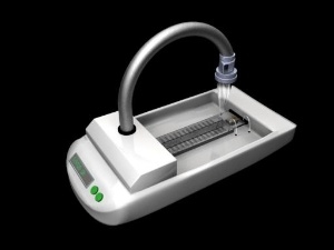 |
| The Patho-ID Chip, designed for the European Defense Agency, will provide rapid, highly sensitive detection of airborne pathogens. (c) NANOIDENT Technologies AG |
Abstract:
Printed Sensors a Key Component of Novel Detection System
NANOIDENT Partners With Life Science and Technology Leaders to Detect Airborne Pathogens for European Defence Agency
LINZ, Austria | Posted on April 16th, 2008NANOIDENT Technologies AG, a leader in the development and manufacture of printed semiconductor-based optoelectronic sensors, today announced the closing of a multi-party agreement with German company microfluidic ChipShop to develop a unique airborne pathogen detection system for the European Defence Agency.
The goal of the project is to develop an autonomous lab-on-a-chip based system, called the PathoID-Chip, for the detection of airborne chemical and biological agents. The system will be able to simultaneously test for multiple pathogens, in a shorter time and with greater sensitivity than is possible with conventional test methods. Tests will be completed in minutes and will be repeated every ten minutes; statistically, this is less time than it should take for a person to become infected. As a result, the presence of harmful substances can be detected in minutes and action can then be taken to reduce exposure.
To achieve these goals, the project combines several novel technologies to collect a sample from the air, inject it into liquid, process it and perform analysis. Other partners in the project include Clemens GmbH, Bundeswehr Institute of Microbiology, Friedrich-Loeffler-Institute, Joanneum Research Forschungsgesellschaft mbH, and Bertin Technologies. NANOIDENT's technology is a core element of the system, and represents a major advance in point-of-use testing. Because optoelectronic sensors are printed onto each chip, the system does not require laboratory handling or bulky, power-hungry, expensive optical readout equipment, making it much more portable, rugged, and tolerant of dust than conventional test systems. The proximity of the sensor to the sample also results in much higher sensitivity than conventional systems.
"Our unique printed sensor technology makes it possible to develop a truly mobile detection system, offering faster detection and minimizing exposure to harmful chemical and biological agents," said Dr. Max Sonnleitner, VP of NANOIDENT's Life Sciences division. "We are proud to contribute a key enabling technology to this innovative project and to be a part of such an outstanding team."
####
About NANOIDENT Technologies AG
NANOIDENT�named by Red Herring as one of the world�s 100 leading technology companies�is the market leader in the development and manufacture of printed semiconductor-based optoelectronic sensors. The company�s core technology merges the latest breakthroughs in materials science and nanotechnology with modern printing techniques to create a new class of semiconductor devices. The revolutionary SEMICONDUCTOR 2.0� Platform is the basis of the world�s first commercial printed photonic sensors, enabling a whole new generation of applications in the industrial, biometric, and life science markets.
NANOIDENT�s high speed, environmentally friendly manufacturing process utilizes liquid nanomaterials and additive production techniques. These liquids are used to print electronic circuits on a wide variety of surfaces, producing products in mere hours for prototype as well as high volume applications. The company�s printed semiconductor devices can be bendable, disposable, light, ultrathin, and large area. They have application specific spectral and electronic properties, and can contain light sources and light detectors as well as electronic circuits. These unique characteristics enable cost-effective, custom designed devices for applications such as industrial, chemical, biological, and biometric sensors.
Privately held, the company is headquartered in Linz, Austria, with subsidiaries in San Francisco, California; Nuremberg, Germany; and Grenoble, France.
For more information, please click here
Contacts:
NANOIDENT Technologies AG
Ulrike Kaiser, +43 732 9024 0
Fax: +43 732 9044 5
www.nanoident.com
or
Schwartz Communications, Inc.
Kristin Amico, + 1-415-512-0770
Copyright © Business Wire 2008
If you have a comment, please Contact us.Issuers of news releases, not 7th Wave, Inc. or Nanotechnology Now, are solely responsible for the accuracy of the content.
Bookmark:


| Related News Press |
News and information
![]() Simulating magnetization in a Heisenberg quantum spin chain April 5th, 2024
Simulating magnetization in a Heisenberg quantum spin chain April 5th, 2024
![]() NRL charters Navy�s quantum inertial navigation path to reduce drift April 5th, 2024
NRL charters Navy�s quantum inertial navigation path to reduce drift April 5th, 2024
![]() Discovery points path to flash-like memory for storing qubits: Rice find could hasten development of nonvolatile quantum memory April 5th, 2024
Discovery points path to flash-like memory for storing qubits: Rice find could hasten development of nonvolatile quantum memory April 5th, 2024
Sensors
Announcements
![]() NRL charters Navy�s quantum inertial navigation path to reduce drift April 5th, 2024
NRL charters Navy�s quantum inertial navigation path to reduce drift April 5th, 2024
![]() Discovery points path to flash-like memory for storing qubits: Rice find could hasten development of nonvolatile quantum memory April 5th, 2024
Discovery points path to flash-like memory for storing qubits: Rice find could hasten development of nonvolatile quantum memory April 5th, 2024
Homeland Security
![]() The picture of health: Virginia Tech researchers enhance bioimaging and sensing with quantum photonics June 30th, 2023
The picture of health: Virginia Tech researchers enhance bioimaging and sensing with quantum photonics June 30th, 2023
![]() Sensors developed at URI can identify threats at the molecular level: More sensitive than a dog's nose and the sensors don't get tired May 21st, 2021
Sensors developed at URI can identify threats at the molecular level: More sensitive than a dog's nose and the sensors don't get tired May 21st, 2021
![]() Highly sensitive dopamine detector uses 2D materials August 7th, 2020
Highly sensitive dopamine detector uses 2D materials August 7th, 2020
Military
![]() NRL charters Navy�s quantum inertial navigation path to reduce drift April 5th, 2024
NRL charters Navy�s quantum inertial navigation path to reduce drift April 5th, 2024
![]() What heat can tell us about battery chemistry: using the Peltier effect to study lithium-ion cells March 8th, 2024
What heat can tell us about battery chemistry: using the Peltier effect to study lithium-ion cells March 8th, 2024
![]() New chip opens door to AI computing at light speed February 16th, 2024
New chip opens door to AI computing at light speed February 16th, 2024
Alliances/Trade associations/Partnerships/Distributorships
![]() Chicago Quantum Exchange welcomes six new partners highlighting quantum technology solutions, from Chicago and beyond September 23rd, 2022
Chicago Quantum Exchange welcomes six new partners highlighting quantum technology solutions, from Chicago and beyond September 23rd, 2022
![]() University of Illinois Chicago joins Brookhaven Lab's Quantum Center June 10th, 2022
University of Illinois Chicago joins Brookhaven Lab's Quantum Center June 10th, 2022
Printing/Lithography/Inkjet/Inks/Bio-printing/Dyes
![]() Presenting: Ultrasound-based printing of 3D materials�potentially inside the body December 8th, 2023
Presenting: Ultrasound-based printing of 3D materials�potentially inside the body December 8th, 2023
![]() Simple ballpoint pen can write custom LEDs August 11th, 2023
Simple ballpoint pen can write custom LEDs August 11th, 2023
![]() Disposable electronics on a simple sheet of paper October 7th, 2022
Disposable electronics on a simple sheet of paper October 7th, 2022
|
|
||
|
|
||
| The latest news from around the world, FREE | ||
|
|
||
|
|
||
| Premium Products | ||
|
|
||
|
Only the news you want to read!
Learn More |
||
|
|
||
|
Full-service, expert consulting
Learn More |
||
|
|
||