Home > Press > SUSS MicroTec Boosts Nanotechnology with New Toolset for Mask Aligners
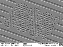 |
| 160nm wide holes positioned in concentric rings as used for photonics crystals. Printed in Amonil MM S4 on a SUSS MA6 Mask Aligner. Source: FhG/IZM |
Abstract:
SUSS MicroTec, supplier of innovative solutions for the 3D, MEMS, Advanced Packaging and Nanotechnology markets, has launched an advanced nanotechnology toolset for its Mask Aligners. The new Nano Imprint Lithography (NIL) tool enables SUSS Aligners to print resist thicknesses from less than 100 nanometers to a few hundred microns with a printing resolution down to a few nanometers.
SUSS MicroTec Boosts Nanotechnology with New Toolset for Mask Aligners
Garching, Germany | Posted on March 3rd, 2008UV-NIL is a low-cost production technology that is based on UV-curing. It has been developed as a cost-effective alternative to high-resolution e-beam lithography to print sub-20 nanometer geometries. UV-NIL applications with promising perspectives include semiconductor, MOEMS, NEMS and optoelectronic technologies.
This toolset can be upgraded on any previously installed SUSS MA6 Mask Aligner with very limited effort. Therefore SUSS MicroTec offers its customers an easy and quick step into the world of Nano.
"Nanotechnology represents a promising new business opportunity for SUSS MicroTec", said Rolf Wolf, General Manager of SUSS MicroTec Lithography division. "With the new UV-NIL tooling for mask aligners, SUSS MicroTec is once again providing market leadership for evolutionary as well as revolutionary innovative processing techniques."
####
About SUSS MicroTec
SUSS MicroTec machines are used by leading semiconductor manufacturers as well as renowned research institutes to make and test state-of-the art microchips and sensors. Many of the products you use in your daily life such as PDA's, GPS systems, cell phones etc. have at sometime been touched by equipment from SUSS MicroTec.
As a global supplier of production and test equipment for the semiconductor and related industries SUSS is especially present in markets including Advanced Packaging, MEMS, Nanotechnology, Compound Semiconductor, Silicon-On-Insulator and 3D Interconnect. Products include precision lithography tools (mask aligners, spin & spray coaters), wafer bonders and test systems.
For more information, please click here
Contacts:
Brigitte Wehrmann
Marketing Communications Manager Lithography Division
SUSS MicroTec Lithography GmbH
Schlei�heimer Str. 90
D 85748 Garching
Phone:+49 89 32007 237
Copyright © SUSS MicroTec
If you have a comment, please Contact us.Issuers of news releases, not 7th Wave, Inc. or Nanotechnology Now, are solely responsible for the accuracy of the content.
Bookmark:


| Related News Press |
News and information
![]() Simulating magnetization in a Heisenberg quantum spin chain April 5th, 2024
Simulating magnetization in a Heisenberg quantum spin chain April 5th, 2024
![]() NRL charters Navy�s quantum inertial navigation path to reduce drift April 5th, 2024
NRL charters Navy�s quantum inertial navigation path to reduce drift April 5th, 2024
![]() Discovery points path to flash-like memory for storing qubits: Rice find could hasten development of nonvolatile quantum memory April 5th, 2024
Discovery points path to flash-like memory for storing qubits: Rice find could hasten development of nonvolatile quantum memory April 5th, 2024
Announcements
![]() NRL charters Navy�s quantum inertial navigation path to reduce drift April 5th, 2024
NRL charters Navy�s quantum inertial navigation path to reduce drift April 5th, 2024
![]() Discovery points path to flash-like memory for storing qubits: Rice find could hasten development of nonvolatile quantum memory April 5th, 2024
Discovery points path to flash-like memory for storing qubits: Rice find could hasten development of nonvolatile quantum memory April 5th, 2024
Tools
![]() Ferroelectrically modulate the Fermi level of graphene oxide to enhance SERS response November 3rd, 2023
Ferroelectrically modulate the Fermi level of graphene oxide to enhance SERS response November 3rd, 2023
![]() The USTC realizes In situ electron paramagnetic resonance spectroscopy using single nanodiamond sensors November 3rd, 2023
The USTC realizes In situ electron paramagnetic resonance spectroscopy using single nanodiamond sensors November 3rd, 2023
Photonics/Optics/Lasers
![]() With VECSELs towards the quantum internet Fraunhofer: IAF achieves record output power with VECSEL for quantum frequency converters April 5th, 2024
With VECSELs towards the quantum internet Fraunhofer: IAF achieves record output power with VECSEL for quantum frequency converters April 5th, 2024
![]() Nanoscale CL thermometry with lanthanide-doped heavy-metal oxide in TEM March 8th, 2024
Nanoscale CL thermometry with lanthanide-doped heavy-metal oxide in TEM March 8th, 2024
![]() Optically trapped quantum droplets of light can bind together to form macroscopic complexes March 8th, 2024
Optically trapped quantum droplets of light can bind together to form macroscopic complexes March 8th, 2024
![]() HKUST researchers develop new integration technique for efficient coupling of III-V and silicon February 16th, 2024
HKUST researchers develop new integration technique for efficient coupling of III-V and silicon February 16th, 2024
|
|
||
|
|
||
| The latest news from around the world, FREE | ||
|
|
||
|
|
||
| Premium Products | ||
|
|
||
|
Only the news you want to read!
Learn More |
||
|
|
||
|
Full-service, expert consulting
Learn More |
||
|
|
||