Home > Press > Surface Metrology Benefits from Longer Travel Nanopositioning Stages
 |
Abstract:
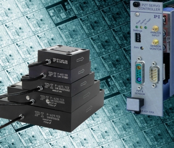
PI (Physik Instrumente) L.P., a leading manufacturer of nanopositioning and precision motion-control equipment semiconductor and photonics applications, has extended its PIHera® family of flexure-guided piezo nanopositioning stages, now offering record travel ranges to 1.8 mm.
Surface Metrology Benefits from Longer Travel Nanopositioning Stages
Auburn, MA | Posted on February 27th, 2008New Stages Capture 200X Larger Areas than Conventional Stages
These precision closed-loop flexure-guided stages can be used for scanning probe applications (surface metrology) and static positioning. Due to the long travel ranges they can scan areas more than 200 times larger than conventional piezo stages with typical ranges of 100x100 µm. Most PIHera® stages provide sub-nanometer resolution and even the 1.8 mm versions achieve 3 nm resolution in closed-loop operation. The compact size is achieved with a new, friction-free and extremely stiff flexure system, which also provides fast response and excellent guiding accuracy. Trajectory precision is in the low-nanometer range. High acceleration forces are provided by patented, long-life multilayer piezoelectric linear actuators. The ability to control motion with millisecond responsiveness and nanometer precision over long travel ranges makes PIHera® stages ideal for measuring and QA applications.
Capacitive Feedback Offers Greater Motion Linearity
The stages are equipped with non-contact capacitive-sensors and provide extremely linear motion with up to 99.98% accuracy and effective resolution in the sub-nanometer range. PI capacitive sensors are absolute-measuring, direct-metrology devices that boast very high bandwidth and exhibit no periodic errors.
Typical Applications
Surface Metrology, Quality Assurance, Scanning Probe Microscopy, Nanometrology, Interferometry, Nanopositioning, Nano-Alignment / Semiconductor Technology
Features & Advantages
- No Wear & Tear: Flexures, Actuators and Sensors are Maintenance-Free
- Longer Lifetime with Patented, Ceramic-Encapsulated Piezo Actuators
- X, XY, Z and XYZ Versions Available
- 50 to 1800 µm Travel Ranges, Nanometer Resolution
- Closed-Loop Digital & Analog Control for Up to 99.98 % Position Accuracy
- Vacuum-Compatible Versions
- Stiff and Compact Design for Millisecond Responsiveness
- Frictionless, Maintenance-Free, Precision Flexure Guiding System
- Direct-Metrology Sensors for Faster Servo Response
Flexible Controllers: High Speed, Digital and Analog Control
A variety of ultra-low-noise controllers with both digital and analog input provide fast communications and come with a wide selection of software tools.
####
About PI (Physik Instrumente) L.P.
PI is a leading manufacturer of precision motion-control equipment for photonics, bio-nanotechnology & semiconductor applications. PI has been developing and manufacturing standard & custom precision products with piezoceramic and electromagnetic drives for 35+ years. The company has been ISO 9001 certified since 1994 and provides innovative, high-quality solutions for OEM and research. PI is present worldwide with eight subsidiaries and total staff of 450+.
For more information, please click here
Contacts:
USA / Canada:
East: David Rego
Tel: (508) 832-3456
Fax: (508) 832-0506
West David Steinberg
Tel: (949) 679-9191
Fax: (949) 679-9292
Europe:
Germany: +49 (721) 4846-0
Italy: +39 (02) 665 011 01
France: +33 (1) 481 039 30
UK: +44 (1582) 764 334
Asia
Japan: +81 (6) 6304 5605
China +86 (21) 687 900 08
Stefan Vorndran
Dir. Corp. Product Marketing & Communications
-----------------------------
PI (Physik Instrumente) L.P.
16 Albert St.
Auburn, MA 01501
Tel: 508-832-3456,
Fax: 508-832-0506
www.pi.ws
www.pi-usa.us
Copyright © PI (Physik Instrumente) L.P.
If you have a comment, please Contact us.Issuers of news releases, not 7th Wave, Inc. or Nanotechnology Now, are solely responsible for the accuracy of the content.
Bookmark:


| Related News Press |
News and information
![]() Simulating magnetization in a Heisenberg quantum spin chain April 5th, 2024
Simulating magnetization in a Heisenberg quantum spin chain April 5th, 2024
![]() NRL charters Navy’s quantum inertial navigation path to reduce drift April 5th, 2024
NRL charters Navy’s quantum inertial navigation path to reduce drift April 5th, 2024
![]() Discovery points path to flash-like memory for storing qubits: Rice find could hasten development of nonvolatile quantum memory April 5th, 2024
Discovery points path to flash-like memory for storing qubits: Rice find could hasten development of nonvolatile quantum memory April 5th, 2024
Announcements
![]() NRL charters Navy’s quantum inertial navigation path to reduce drift April 5th, 2024
NRL charters Navy’s quantum inertial navigation path to reduce drift April 5th, 2024
![]() Discovery points path to flash-like memory for storing qubits: Rice find could hasten development of nonvolatile quantum memory April 5th, 2024
Discovery points path to flash-like memory for storing qubits: Rice find could hasten development of nonvolatile quantum memory April 5th, 2024
Tools
![]() Ferroelectrically modulate the Fermi level of graphene oxide to enhance SERS response November 3rd, 2023
Ferroelectrically modulate the Fermi level of graphene oxide to enhance SERS response November 3rd, 2023
![]() The USTC realizes In situ electron paramagnetic resonance spectroscopy using single nanodiamond sensors November 3rd, 2023
The USTC realizes In situ electron paramagnetic resonance spectroscopy using single nanodiamond sensors November 3rd, 2023
|
|
||
|
|
||
| The latest news from around the world, FREE | ||
|
|
||
|
|
||
| Premium Products | ||
|
|
||
|
Only the news you want to read!
Learn More |
||
|
|
||
|
Full-service, expert consulting
Learn More |
||
|
|
||