Home > Press > Nokia and University of Cambridge launch the Morph - a nanotechnology concept device
 |
Abstract:
Morph, a joint nanotechnology concept, developed by Nokia Research Center (NRC) and the University of Cambridge (UK) - was launched today alongside the "Design and the Elastic Mind" exhibition, on view from February 24 to May 12, 2008, at The Museum of Modern Art (MoMA) in New York. Morph features in both the exhibition catalog and on MoMA's official website.
Nokia and University of Cambridge launch the Morph - a nanotechnology concept device
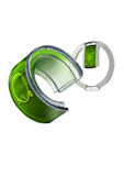
New York, US and Espoo, Finland | Posted on February 25th, 2008Morph is a concept that demonstrates how future mobile devices might be stretchable and flexible, allowing the user to transform their mobile device into radically different shapes. It demonstrates the ultimate functionality that nanotechnology might be capable of delivering: flexible materials, transparent electronics and self-cleaning surfaces. Dr. Bob Iannucci, Chief Technology Officer, Nokia, commented: "Nokia Research Center is looking at ways to reinvent the form and function of mobile devices; the Morph concept shows what might be possible".
Dr. Tapani Ryhanen, Head of the NRC Cambridge UK laboratory, Nokia, commented: "We hope that this combination of art and science will showcase the potential of nanoscience to a wider audience. The research we are carrying out is fundamental to this as we seek a safe and controlled way to develop and use new materials."
Professor Mark Welland, Head of the Department of Engineering's Nanoscience Group at the University of Cambridge and University Director of Nokia-Cambridge collaboration added: "Developing the Morph concept with Nokia has provided us with a focus that is both artistically inspirational but, more importantly, sets the technology agenda for our joint nanoscience research that will stimulate our future work together."
The partnership between Nokia and the University of Cambridge was announced in March, 2007 - an agreement to work together on an extensive and long term programme of joint research projects. NRC has established a research facility at the University's West Cambridge site and collaborates with several departments - initially the Nanoscience Center and Electrical Division of the Engineering Department - on projects that, to begin with, are centered on nanotechnology.
Elements of Morph might be available to integrate into handheld devices within 7 years, though initially only at the high-end. However, nanotechnology may one day lead to low cost manufacturing solutions, and offers the possibility of integrating complex functionality at a low price.
For further information, please visit the websites www.moma.org/elasticmind and www.nokia.com/A4126514
About Nokia Research Center
Nokia Research Center (NRC) looks beyond Nokia's existing business and product development to challenge current strategies and to stimulate renewal in the company's direction. Working closely with all Nokia business units, NRC's research explores new frontiers in digital services, physical-digital connections, human interaction, data and content technologies, device architecture, and access and connectivity. NRC promotes open innovation by working on research projects in collaboration with universities and research institutes around the world.
####
About Nokia
Nokia is the world leader in mobility, driving the transformation and growth of the converging Internet and communications industries. Nokia makes a wide range of mobile devices and provides people with experiences in music, navigation, video, television, imaging, games and business. Nokia also provides equipment, solutions and services for communications networks.
About the University of Cambridge
The University of Cambridge will celebrate its 800th anniversary in 2009. It is one of the finest universities in the world, a superb British university with global reach. It is renowned for its 31 colleges and world class teaching departments, ground breaking research and breathtaking architecture. It attracts the very best and brightest students, regardless of background, and offers one of the UK's most generous bursary schemes.
Cambridge was recently ranked number two in the world and the number one University outside the US, in two separate surveys, the Shanghai Jiao Tong University 2006 survey, and in the Times Higher Education magazine's world rankings.
Cambridge people have been awarded more Nobel Prizes than those from any other UK university with more than 80 laureates.
The Nanoscience Centre is an 1800m� research facility completed in January 2003 and located at the north east corner of the University's West Cambridge Site. The Centre provides open access to over 300 researchers from a variety of University Departments to the nanofabrication and characterisation facilities housed in a combination of Clean Rooms and low noise laboratories. Office space is primarily home to the Department of Engineering's Nanoscience Group, technical and administrative staff and members of other research groups who require long term access to facilities. www.nanoscience.cam.ac.uk
The Electrical Engineering Division of the Department of Engineering is housed in a purpose-built laboratory in the University's West Cambridge site that was opened in January 2006 that includes a 650 m2 clean facility, dark rooms, chemical laboratories and electronics labs. It builds on Cambridge's history of world-leading research in Photonics and Electronics by significantly enhancing collaboration with industry and by providing a focus for multidisciplinary research involving over 200 engineers, as well as chemists, physicists, materials scientists and bioscientists. It includes the 'Centre for Advanced Photonics and Electronics' and the 'Cambridge Integrated Knowledge Centre for Advanced Manufacturing Technologies for Photonics and Electronics'. www.eng.cam.ac.uk/research/div-b/divhomeB.shtml
For more information, please click here
Contacts:
Nokia
Communications, Corporate Development Office
Tel. +358 7180 69472
E-mail:
Nokia
Communications
Tel. +358 7180 34900
E-mail:
Genevieve Maul
University of Cambridge
Office of Communications
Tel. +44 1223 332 3000
Mobile: +44 7774 017 464
Copyright © Nokia
If you have a comment, please Contact us.Issuers of news releases, not 7th Wave, Inc. or Nanotechnology Now, are solely responsible for the accuracy of the content.
Bookmark:


| Related News Press |
News and information
![]() Simulating magnetization in a Heisenberg quantum spin chain April 5th, 2024
Simulating magnetization in a Heisenberg quantum spin chain April 5th, 2024
![]() NRL charters Navy�s quantum inertial navigation path to reduce drift April 5th, 2024
NRL charters Navy�s quantum inertial navigation path to reduce drift April 5th, 2024
![]() Discovery points path to flash-like memory for storing qubits: Rice find could hasten development of nonvolatile quantum memory April 5th, 2024
Discovery points path to flash-like memory for storing qubits: Rice find could hasten development of nonvolatile quantum memory April 5th, 2024
Announcements
![]() NRL charters Navy�s quantum inertial navigation path to reduce drift April 5th, 2024
NRL charters Navy�s quantum inertial navigation path to reduce drift April 5th, 2024
![]() Discovery points path to flash-like memory for storing qubits: Rice find could hasten development of nonvolatile quantum memory April 5th, 2024
Discovery points path to flash-like memory for storing qubits: Rice find could hasten development of nonvolatile quantum memory April 5th, 2024
Human Interest/Art
![]() Drawing data in nanometer scale September 30th, 2022
Drawing data in nanometer scale September 30th, 2022
![]() Scientists prepare for the world�s smallest race: Nanocar Race II March 18th, 2022
Scientists prepare for the world�s smallest race: Nanocar Race II March 18th, 2022
![]() Graphene nanotubes revolutionize touch screen use for prosthetic hands August 3rd, 2021
Graphene nanotubes revolutionize touch screen use for prosthetic hands August 3rd, 2021
![]() JEOL Announces 2020 Microscopy Image Grand Prize Winners January 7th, 2021
JEOL Announces 2020 Microscopy Image Grand Prize Winners January 7th, 2021
Events/Classes
![]() Researchers demonstrate co-propagation of quantum and classical signals: Study shows that quantum encryption can be implemented in existing fiber networks January 20th, 2023
Researchers demonstrate co-propagation of quantum and classical signals: Study shows that quantum encryption can be implemented in existing fiber networks January 20th, 2023
Alliances/Trade associations/Partnerships/Distributorships
![]() Chicago Quantum Exchange welcomes six new partners highlighting quantum technology solutions, from Chicago and beyond September 23rd, 2022
Chicago Quantum Exchange welcomes six new partners highlighting quantum technology solutions, from Chicago and beyond September 23rd, 2022
![]() University of Illinois Chicago joins Brookhaven Lab's Quantum Center June 10th, 2022
University of Illinois Chicago joins Brookhaven Lab's Quantum Center June 10th, 2022
|
|
||
|
|
||
| The latest news from around the world, FREE | ||
|
|
||
|
|
||
| Premium Products | ||
|
|
||
|
Only the news you want to read!
Learn More |
||
|
|
||
|
Full-service, expert consulting
Learn More |
||
|
|
||