Home > Press > Debut of TEAM 0.5, the World's Best Microscope
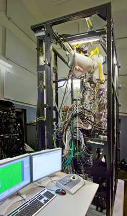 |
| TEAM 0.5, the world's best transmission electron microscope, is being assembled at the National Center for Electron Microscopy. (Photo Roy Kaltschmidt, Berkeley Lab CSO) |
Abstract:
TEAM 0.5, the world's most powerful transmission electron microscope — capable of producing images with half‑angstrom resolution (half a ten-billionth of a meter), less than the diameter of a single hydrogen atom — has been installed at the Department of Energy's National Center for Electron Microscopy (NCEM) at Lawrence Berkeley National Laboratory.
Debut of TEAM 0.5, the World's Best Microscope
Berkeley, CA | Posted on January 22nd, 2008"We have beam down the column," announced Uli Dahmen of Berkeley Lab's Materials Sciences Division, who is head of NCEM and director of DOE's collaborative TEAM Project, when the TEAM 0.5 microscope first delivered its ultrabright electron beam at Berkeley Lab in late December.
The TEAM Project (TEAM stands for Transmission Electron Aberration-corrected Microscope) is led by Berkeley Lab in a collaboration with DOE's Argonne and Oak Ridge National Laboratories, the Frederick Seitz Materials Laboratory of the University of Illinois, and two private companies specializing in electron microscopy, the FEI Company headquartered in Portland, Oregon, and CEOS of Heidelberg, Germany.
Now that TEAM 0.5's basic systems are operational, additional components and facilities are being completed and tuned, including a state-of-the-art control room display that shows the sample under the microscope on a flat panel resembling a wide-screen, high-definition TV. After a long series of rigorous tests and adjustments, TEAM 0.5 will become available to outside users by October, 2008.
Atom by atom in 3-D
In preliminary tests at the FEI Company, before the TEAM 0.5 was shipped, NCEM's Christian Kisielowski tested the microscope's ability to resolve individual atoms and precisely locate their positions in three dimensions. He made a series of images of two gold crystals connected by a "nanobridge" only a few dozen atoms wide. From each exposure to the next, individual gold atoms could be seen changing positions.
To achieve this extraordinary resolution, TEAM 0.5 embodies technical advances that have only recently become possible, including ultra-stable electronics, improved aberration correctors, and an extremely bright electron source.
Spherical aberration degrades images, making points of light look like disks, and correcting it can make dramatic improvements to image resolution. (This was famously demonstrated in 1993, when spherical aberration in the Hubble Space Telescope's optical lenses was corrected in a special space mission.) In the case of electron microscopes, a series of multipole magnetic lenses of varying geometries shapes the electron beam.
"Correcting spherical aberration in an electron microscope has long been possible in theory," says Dahmen. "But only recently has it become practical, because today's stable electronics reduce drift and fast computers allow continuous adjustments in real time." Corrector technology has even become available commercially, says Dahmen, "but no off-the-shelf corrector can match TEAM 0.5's ability to compensate even higher-order aberrations."
Correcting spherical aberration makes it possible to use the TEAM 0.5 not only for broad-beam, "wide-angle" images but also for scanning transmission electron microscopy (STEM), in which the tightly focused electron beam is moved across the sample as a probe, capable of performing spectroscopy on one atom at a time — an ideal way to precisely locate impurities in an otherwise homogeneous sample, such as individual dopant atoms in a semiconductor material.
Aberration correction is also essential for another advanced feature of TEAM 0.5: its ability to maintain high resolution with lower electron beam energies.
"Low energy electrons have longer wavelengths, so they are harder to focus," Dahmen explains. "Aberration correction allows better than one-angstrom resolution with excellent contrast even at 80 kilovolts. This is important when you don't want to damage the sample with a high-energy beam — in biological studies, for example."
It's not just high resolution that makes TEAM 0.5 the world's best microscope, Dahmen says. When all the electrons in the beam focus at the same plane, image contrast and signal-to-noise ratio improve tremendously.
"It's because the signal-to-noise ratio is so good that you can adjust focus atom by atom, with enough sensitivity to obtain information about the three-dimensional atomic structure of a single nanoparticle." Dahmen adds, "This brings us within reach of meeting the great challenge posed by the famous physicist Richard Feynman in 1959: the ability to analyze any chemical substance simply by looking to see where the atoms are."
The position of individual atoms in a structure can be determined by taking images at different angles, from which the computer reconstructs a 3-D tomograph of the sample, as in a CAT scan. To make this possible an innovative system capable of tilting and rotating the sample, and moving it up, down, or sideways under the electron beam, is also being developed at NCEM.
Much smaller than sample stages now in use, the new TEAM stage will be housed entirely inside the microscope column. Manipulating the sample by such methods as minute piezoelectric "crawlers" that change shape when electricity is applied, the new stage will be able to control and reproduce the sample's position and attitude with an accuracy of less than a billionth of a meter.
Installation of the new stage must await the next phase of the TEAM Project: the TEAM I microscope, due to be set up at NCEM early in 2009.
While TEAM 0.5 corrects spherical aberration in both the "probe" beam (the electron beam before it strikes the sample) and the image beam (after it exits the sample, but before it reaches the detector), TEAM I will also correct chromatic aberration in the image beam, which has never beeen accomplished before. Spherical aberration is caused by the shape of a lens; chromatic aberration results when a lens refracts light or electrons of different wavelengths (different colors or energies) at different angles.
"Correcting chromatic aberration is harder and takes more space," says Dahmen. "The chromatic aberration corrector will add two feet to the height of the TEAM I column. But the new configuration will also allow us to enlarge the gap between the pole pieces, into which the sample fits. In TEAM 0.5 this gap is only about two millimeters, so we have to use traditional outside-mounted sample stages, with limited space to manipulate the sample. In TEAM I the gap will be five millimeters; the sample stage will have much greater freedom of movement."
New vistas in the realm of the small
TEAM 0.5 and TEAM I will be housed side by side at NCEM for some time, occupying the two multistory "silos" that until recently were the homes of the historic High-Voltage Electron Microscope and the Atomic Resolution Microscope, the most powerful microscopes in the world when NCEM was established in the early 1980s.
Ambitious as those microscopes were in their day, says TEAM's Project Manager, Peter Denes of the Engineering Division, "when the TEAM Project was launched in 2004, it was not quite clear if the goals could even be achieved. The electron microscopy community had never done a collaborative project like TEAM before, and certainly not with full DOE project-management rigor."
Says Denes, "Perhaps the biggest contributor to success was a series of scientific workshops that contributed to forming a converging opinion on what the next steps would be, and what would constitute success. That helped in getting everyone — if not quite on the same page — at least in the same book."
Dahmen agrees. "This is a big jump for the microscopy community. TEAM's success will open the door to other ambitious developments around the world."
Dahmen suggests at least two broad categories of researchers who will benefit from the powerful new electron microscopes: experts with sophisticated microscopy problems to solve, and scientists less familiar with electron microscopy but with a particular problem for which microscopy can provide the answer.
"For example, Jim Zuo at the University of Illinois is doing studies of electron diffraction from the surface of single nanoparticles," Dahmen says. "He sees evidence of surface contraction. But when we at NCEM do imaging of similar nanoparticles, we find that the surface is expanding. Jim looks forward to using the TEAM microscope because it can do diffraction and imaging of the same particle at the same time — a grand experiment, and the only way to solve the apparent contradiction."
An example of a problem-solving nonspecialist, says Dahmen, might be a materials scientist who has created a new kind of nanostructure, such as a tetrapod semiconductor, and needs to know exactly where in this complex, three-dimensional shape the impurity atoms reside. "TEAM's ability to image the structure in 3-D through tomography and its ability to do spectroscopy with single-atom sensitivity can identify each kind of atom at each position in the structure. That has never been possible before."
The basic TEAM components of aberration correction, enhanced signal-to-noise ratio, single-atom sensitivity, and an ultrabright beam that can be used in both TEM and STEM modes — all the while manipulating the sample in the beam — are goals that until recently seemed at the very edge of technological daring. All are on track, and some have been solved ahead of schedule. The TEAM Project's continuing success, signaled by the installation of TEAM 0.5 at NCEM, has opened the possibility of numerous future advances in electron microscopy that were barely conceivable when TEAM was launched.
The multi-institutional TEAM project represents a new kind of distributed planning and cooperation for the electron microscope community, moving beyond the limited, incremental improvements of individual investigators and harnessing the power of collaboration. Argonne National Laboratory is leading the development of the chromatic-aberration corrector in close collaboration with CEOS in Heidelberg. The University of Illinois's Frederick Seitz Materials Laboratory is jointly developing the new piezoelectric-controlled sample stage with Berkeley Lab's NCEM, and Oak Ridge National Laboratory is helping to optimize the new probe corrector. NCEM acts as project leader to integrate the individual components into single instruments, in close collaboration with all other TEAM partners. The TEAM Project is supported by the U.S. Department of Energy's Office of Science. For more about the TEAM Project, visit http://ncem.lbl.gov/TEAM-project/ .
####
About Berkeley Lab
Berkeley Lab is a U.S. Department of Energy national laboratory located in Berkeley, California. It conducts unclassified scientific research and is managed by the University of California. Visit our website at http://www.lbl.gov .
For more information, please click here
Contacts:
Paul Preuss
(510) 486-6249
Copyright © Berkeley Lab
If you have a comment, please Contact us.Issuers of news releases, not 7th Wave, Inc. or Nanotechnology Now, are solely responsible for the accuracy of the content.
Bookmark:


| Related News Press |
News and information
![]() Simulating magnetization in a Heisenberg quantum spin chain April 5th, 2024
Simulating magnetization in a Heisenberg quantum spin chain April 5th, 2024
![]() NRL charters Navy’s quantum inertial navigation path to reduce drift April 5th, 2024
NRL charters Navy’s quantum inertial navigation path to reduce drift April 5th, 2024
![]() Discovery points path to flash-like memory for storing qubits: Rice find could hasten development of nonvolatile quantum memory April 5th, 2024
Discovery points path to flash-like memory for storing qubits: Rice find could hasten development of nonvolatile quantum memory April 5th, 2024
Imaging
![]() Nanoscale CL thermometry with lanthanide-doped heavy-metal oxide in TEM March 8th, 2024
Nanoscale CL thermometry with lanthanide-doped heavy-metal oxide in TEM March 8th, 2024
Laboratories
![]() A battery’s hopping ions remember where they’ve been: Seen in atomic detail, the seemingly smooth flow of ions through a battery’s electrolyte is surprisingly complicated February 16th, 2024
A battery’s hopping ions remember where they’ve been: Seen in atomic detail, the seemingly smooth flow of ions through a battery’s electrolyte is surprisingly complicated February 16th, 2024
![]() NRL discovers two-dimensional waveguides February 16th, 2024
NRL discovers two-dimensional waveguides February 16th, 2024
Announcements
![]() NRL charters Navy’s quantum inertial navigation path to reduce drift April 5th, 2024
NRL charters Navy’s quantum inertial navigation path to reduce drift April 5th, 2024
![]() Discovery points path to flash-like memory for storing qubits: Rice find could hasten development of nonvolatile quantum memory April 5th, 2024
Discovery points path to flash-like memory for storing qubits: Rice find could hasten development of nonvolatile quantum memory April 5th, 2024
Tools
![]() Ferroelectrically modulate the Fermi level of graphene oxide to enhance SERS response November 3rd, 2023
Ferroelectrically modulate the Fermi level of graphene oxide to enhance SERS response November 3rd, 2023
![]() The USTC realizes In situ electron paramagnetic resonance spectroscopy using single nanodiamond sensors November 3rd, 2023
The USTC realizes In situ electron paramagnetic resonance spectroscopy using single nanodiamond sensors November 3rd, 2023
|
|
||
|
|
||
| The latest news from around the world, FREE | ||
|
|
||
|
|
||
| Premium Products | ||
|
|
||
|
Only the news you want to read!
Learn More |
||
|
|
||
|
Full-service, expert consulting
Learn More |
||
|
|
||