Home > Press > Highlights of the IVAM Product Market “Micro, Nano & Materials” at MicroTechnology/HANNOVER MESSE
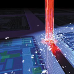 |
| 3D animation picture showing the water jet guided laser beam, used for dicing a wafer. Source: SYNOVA S.A. |
Abstract:
April 21-25, 2008, hall 6/booth F16
IVAM joint pavilion as outstanding competence center for microtechnology, nanotechnology and advanced materials
Highlights of the IVAM Product Market “Micro, Nano & Materials” at MicroTechnology/HANNOVER MESSE
HANNOVER, Germany | Posted on January 17th, 2008The visitors of the trade fair MicroTechnology within HANNOVER MESSE 2008 can expect solutions for a broad range of product miniaturization questions on the Product Market "Micro, Nano & Materials", organized by IVAM Microtechnology Network. "With over 60 exhibitors, the IVAM joint pavilion is one of the largest competence centers in Europe - and even in the world," stresses Manfred Kutzinski, project manager MicroTechnology of Deutsche Messe, in the magazine Lasermarkt in early 2008.
A special exhibition called "Laser for micro machining" as a part of the Product Market introduces innovative methods and laser applications for highly precise production. Japan, the partner country of this year's HANNOVER MESSE, will also be represented at the IVAM booth. On April 22, the forum "Innovations for Industry" will focus on Japan. On the forum there will also be the Laser Day on Wednesday, April 23, when the program will be dedicated exclusively to the topic laser technology.
Microfluidics
Bartels Mikrotechnik GmbH presents a new method for fluid transport called Electrowetting. An electric field changes the surface properties, for instance of a lab-on-a-chip, in a way that sample drops can be moved in a desired direction. This, for the first time, would enable a lab-on-a-chip without any structures.
Also the latest generation of the Bartels micropump will be exhibited. By using a double actuator, the mp6 pump is achieving up to 500 mbars of pressure while a new drive signal makes pumping noiseless. Also self-priming and gas-bubble-tolerance are improved significantly. "The basic principle of the piezo membrane pump is simple, so an adaptation to manifold requirements is possible", illustrates product manager Severin Dahms, "Whether a larger flow range, certain material demands, or higher flow accuracy - the customer decides."
Micronit Microfluidics b.v. will show its new microfluidic connection platform. "A major challenge commonly encountered in microfluidics technology is the tedious replacement of devices. Micronit offers a platform tool that makes it possible to attach a microfluidic device to any instrument in a matter of seconds", Ronny van‘t Oever, CTO of Micronit, explains.
Micro actuators
Linear and rotary movements can be produced directly and with a finely adjustable speed by the Elliptec Motor. It is small, light and suitable for servo tasks in consumer goods, optics, industrial and medical fields as well as for vacuum applications. To simplify the integration of a piezo drive in an application, Elliptec Resonant Actuator AG developed a module solution, which combines the Elliptec Motor, the driven element, and the electronics in one compact housing. Through various software versions the modules can, depending on the application, rather be similar to a DC motor or a step motor, but with significantly enhanced functionality.
Smallest parts
Servometer Precision Manufacturing Group, LLC manufactures custom miniature electrodeposited nickel metal bellows and bellows assemblies, bellows type flexible shaft couplings, gold plated bellows contacts, and electroforms. The bellows are as small as 0.020" in diameter and can be used as springs and flexible seals. Bellows type flexible shaft couplings can accommodate axial, angular and offset deflections with zero backlash and low windup. Gold plated contact bellows can be used in delicate electronic applications where good contact and continuity are important.
Smallest functionalized parts for many different industrial sectors like medical technology, sensor technology, microfluidics or drive technology will be exhibited by the Fraunhofer Institute for Manufacturing Technology and Applied Materials Research (IFAM). The combination of the economic serial process metal injection molding with further powder based processes - printing of metal structures or usage of nanocomposites - leads to micro parts with a high integration of functionality.
"We are able to produce single items or small production runs with a high added value. Plus, the quantity of swarf is only a few kilos each year", says Paul Rolland, General Manager of the PRF Group of which STEEC, a company which specializes in precision micromechanics, is a member. "Our products are found, for example, within analytical equipment used in particle accelerators or for taking physical measurements on a molecular level. We also produce component parts for wave guides that are used to capture the low levels of electro-magnetic energy coming from the cosmos", explains Rolland. The micron is the unit of scale on which STEEC works daily with many metals including stainless steels, copper and various alloys.
Micro production - with or without laser
The precision and reliability requirements in laser material processing are becoming more and more demanding. JENOPTIK Laser, Optik, Systeme GmbH present its newly developed F-Theta JENar lenses for 532 and 1,064 nm for large beam diameters and large scan field sizes at the IVAM joint pavilion. In addition to the manufacturing of standard products in a compact modular construction for the integration in existing systems, JENOPTIK also produces individual UV-lenses and optical laser components.
JENOPTIK also showcases its HEX04 hot embossing/nano imprinting system. It has been created to provide a large volume manufacturing solution for a wide range of microoptical and microfluidical applications. The HEX04 uses JENOPTIK´s proprietary "Active De-Embossing Technology" which ensures an effective separation process of the embossing molds from the substrate.
A hand-welding laser system for prototype manufacturing and small series is presented by Rofin / Baasel Lasertech. Visitors can also see and try a compact desk device for the marking of several materials. The experts from Rofin furthermore answer questions concerning laser processing of non-metallic materials. Carbon dioxide laser sources with a power range of up to 2,500 Watts cut for example polymer sheets, which are used as test tapes in the medical device technology. They are also optimal for applications in the field of forgery-safety, for example the complex perforation of identity documents. Even eggshells can be scribed for easy opening. A catering company thus avoids contamination by fragments of broken eggshells.
For the first time a high-power-diode laser line is used for the processing of thin film solar cells on glass substrates. The laser module by LIMO Lissotschenko Mikrooptik GmbH provides 350 W in a 12 x 0.1 mm line. Two key features of the laser are high power density and homogeneous power distribution along the line. These properties enable the processing of seed layers of amorphous silicon as well as the growth of carbon-silicon.
Synova S.A.'s Laser MicroJet technology is a hybrid cutting process where a hair-thin water jet guides a laser beam on to the work piece. Contrary to standard cutting methods, Laser MicroJet uses water to cool the material surface for optimal protection against thermal damage, as well as to create a natural layer to prevent deposition or contamination.
The Institute of Production Engineering of the Helmut-Schmidt-University in Hamburg introduces projects in the research fields micro manufacturing, robotics and production automation. Main objective in the research area micro production is the determination of physical size effects arising from down scaling manufacturing processes and their inline compensation. Based on fundamental research the department develops and transfers technical solutions into industrial application.
Nanotechnology: special films and polishing media
nanoFlexx GmbH has cooperated with the Fraunhofer Institute for Silicon Technology ISIT to develop a process to produce micro and nano structures on special films at low cost. There is a booming market available for such wide web films: solar panels that show self-cleaning effects at rainy or windy conditions, automobile headlights that improve the visible area on the road using light-guiding and micro-structured films or decorative products with holographic structures on the surface to improve the optical characteristics are only a few examples.
"The products of nanoFlexx are very useful to achieve a self-cleaning effect, an improved visibility, anti-reflexion properties, light guidance or to reduce friction and adhesion", explains Managing Director Haroun Malik.
The core business of NanoCompound GmbH is ultra-precision polishing media. Smoothness values in the order of Ĺngstroms are achieved. The nano diamond material Fullaron is used as an additive to improve material and surface properties. Here the topics are for example scratch and wear-resistant surfaces, long-lasting mat lacquers, low-friction tribological systems, heat conduction systems, improved plastics and ultra thin coatings.
Surface analysis
NanoFocus AG presents 3D measurement methods for surface inspection in the quality assurance process. In particular, the confocal 3D measurement, for example with the microscope μsurf explorer, is adapted optimally for measuring topography and roughness in laboratories and the production process. With the μsurf explorer, NanoFocus offers a complete package including the software μsoft analysis for the first time. NanoFocus systems are already used for the monitoring of surfaces in the automotive, steel and printing industries.
Fries Research & Technology GmbH, a provider of equipment and systems for the non-destructive analysis of material surfaces, presents the confocal microscope MicroSpy Topo and new fully-automated measurement systems for the front-end range of semiconductor and MEMS product manufacturers. The MicroSpy Topo was designed as a beginners' system for applications in research and development as well as production. The highly complex systems of the series MFE (Metrology for Frontend), however, have high-end features such as multi-sensor technology, automation and robotics handling.
Sensor technology
The Fraunhofer Institute for Silicon Technology ISIT develops in collaboration with Sensordynamics miniaturized, high-precision acceleration and angular rate sensors (gyroscopes) for the automotive industry. A gyroscope detects the movement of a body in space. For example in a car it can be utilized for vehicle dynamic control systems like ESP. Other applications can be image stabilization for cameras and mobile phones as well as interactive interfaces for game paddles in virtual reality animations.
ISIT manufactures sensor structures in dimensions of a few microns using microsystem technologies in a state of the art semiconductor production line. Included are the integration of electronic circuits for signal evaluation in one package. The electronics also performs signal processing and self testing.
The Axetris Microsystems Division from Leister Process Technologies introduces massflow sensors and infrared sources for gas monitoring. IR Microsystems, subsidiary of Leister Process Technologies, presents compact gas sensors based on tuneable laser diodes. The devices are offered as stand-alone or OEM sub-systems for the continuous monitoring of gases like NH3, O2, CO2 and H2O in industrial safety, process monitoring, medical technology, and others. Microprocessor-driven read-out electronics with digital and analogue data outputs offer industry-standard connectivity.
Software solutions for process development
Process Relations GmbH offers software solutions and consulting services for high-tech industries based on the software suite XperiDesk. The PDES (Process Development Execution System) XperiDesk supports complex manufacturing process development from the initial idea to transfer into production. Especially the market segments semiconductor, MEMS, NEMS, bio-medical and solar apply the software. XperiDesk captures all development results in a structured manner, and allows the reuse of previous results and a selective transfer.
Support for founders
"all micro. The Founders' Contest" is one of three contests arranged by start2grow each year. The objective is to help founders realize their business idea quickly and substantially. For this purpose start2grow offers a coaching concept, comprehensive information, and various contacts to financial capital providers and important institutions.
New location
PHOENIX Dortmund, a new location for innovative technologies, spare time and modern work and life forms, is presented by Wirtschaftsförderung Dortmund/dortmund-project and LEG Stadtentwicklung GmbH & Co.KG. The PHOENIX site, with its excellent connections to freeways and Dortmund airport, provides over 200 hectares space.
Partner country Japan
Japan, the partner country of this year's HANNOVER MESSE, will be represented at the IVAM booth with the Micromachine Center, which stands for companies like Olympus, Omron, Panasonic, Mitsubishi Electric, and many more.
Pictures for editorial use can be requested from Josefine Zucker.
####
About IVAM
As international association of companies and institutes in the field of microtechnology, nanotechnology and advanced materials, IVAM's priorities are to create competitive advantages for our members. Our members have appreciated this for 13 years now. 254 member companies and institutes from 17 countries open up new markets and set standards with the support of IVAM. Companies, Institutes, products, services and contact persons are listed here online as well as in the printed IVAM directory.
For more information, please click here
Contacts:
Josefine Zucker
Emil-Figge-Str. 76
44227 Dortmund
Germany
Phone: +49 (0) 2 31 / 97 42-7089
Fax: +49 (0) 2 31 / 97 42-150
E-mail:
Copyright © IVAM
If you have a comment, please Contact us.Issuers of news releases, not 7th Wave, Inc. or Nanotechnology Now, are solely responsible for the accuracy of the content.
Bookmark:


| Related News Press |
Thin films
![]() Utilizing palladium for addressing contact issues of buried oxide thin film transistors April 5th, 2024
Utilizing palladium for addressing contact issues of buried oxide thin film transistors April 5th, 2024
![]() Understanding the mechanism of non-uniform formation of diamond film on tools: Paving the way to a dry process with less environmental impact March 24th, 2023
Understanding the mechanism of non-uniform formation of diamond film on tools: Paving the way to a dry process with less environmental impact March 24th, 2023
![]() New study introduces the best graphite films: The work by Distinguished Professor Feng Ding at UNIST has been published in the October 2022 issue of Nature Nanotechnology November 4th, 2022
New study introduces the best graphite films: The work by Distinguished Professor Feng Ding at UNIST has been published in the October 2022 issue of Nature Nanotechnology November 4th, 2022
![]() Thin-film, high-frequency antenna array offers new flexibility for wireless communications November 5th, 2021
Thin-film, high-frequency antenna array offers new flexibility for wireless communications November 5th, 2021
Sensors
Announcements
![]() NRL charters Navy’s quantum inertial navigation path to reduce drift April 5th, 2024
NRL charters Navy’s quantum inertial navigation path to reduce drift April 5th, 2024
![]() Discovery points path to flash-like memory for storing qubits: Rice find could hasten development of nonvolatile quantum memory April 5th, 2024
Discovery points path to flash-like memory for storing qubits: Rice find could hasten development of nonvolatile quantum memory April 5th, 2024
Interviews/Book Reviews/Essays/Reports/Podcasts/Journals/White papers/Posters
![]() Simulating magnetization in a Heisenberg quantum spin chain April 5th, 2024
Simulating magnetization in a Heisenberg quantum spin chain April 5th, 2024
![]() Discovery points path to flash-like memory for storing qubits: Rice find could hasten development of nonvolatile quantum memory April 5th, 2024
Discovery points path to flash-like memory for storing qubits: Rice find could hasten development of nonvolatile quantum memory April 5th, 2024
Events/Classes
![]() Researchers demonstrate co-propagation of quantum and classical signals: Study shows that quantum encryption can be implemented in existing fiber networks January 20th, 2023
Researchers demonstrate co-propagation of quantum and classical signals: Study shows that quantum encryption can be implemented in existing fiber networks January 20th, 2023
Alliances/Trade associations/Partnerships/Distributorships
![]() Chicago Quantum Exchange welcomes six new partners highlighting quantum technology solutions, from Chicago and beyond September 23rd, 2022
Chicago Quantum Exchange welcomes six new partners highlighting quantum technology solutions, from Chicago and beyond September 23rd, 2022
![]() University of Illinois Chicago joins Brookhaven Lab's Quantum Center June 10th, 2022
University of Illinois Chicago joins Brookhaven Lab's Quantum Center June 10th, 2022
|
|
||
|
|
||
| The latest news from around the world, FREE | ||
|
|
||
|
|
||
| Premium Products | ||
|
|
||
|
Only the news you want to read!
Learn More |
||
|
|
||
|
Full-service, expert consulting
Learn More |
||
|
|
||