Home > Press > New Paper Reveals Nanoscale Details of Photolithography Process
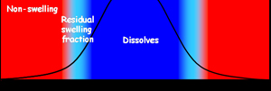 |
| Schematic of the photolithography process shows the formation of a gradient extending from the photoresist material to be removed (center) into the unexposed portions of the resist on the sides. NIST measurements document the residual swelling fraction caused by the developer that can contribute to roughness in the final developed image.
Credit: NIST |
Abstract:
Scientists at the National Institute of Standards and Technology (NIST) have made the first direct measurements of the infinitesimal expansion and collapse of thin polymer films used in the manufacture of advanced semiconductor devices. It's a matter of only a couple of nanometers, but it can be enough to affect the performance of next-generation chip manufacturing. The NIST measurements, detailed in a new paper,* offer a new insight into the complex chemistry that enables the mass production of powerful new integrated circuits.
New Paper Reveals Nanoscale Details of Photolithography Process
GAITHERSBURG, MD | Posted on December 12th, 2007The smallest critical features in memory or processor chips include transistor "gates." In today's most advanced chips, gate length is about 45 nanometers, and the industry is aiming for 32-nanometer gates. To build the nearly one billion transistors in modern microprocessors, manufacturers use photolithography, the high-tech, nanoscale version of printing technology. The semiconductor wafer is coated with a thin film of photoresist, a polymer-based formulation, and exposed with a desired pattern using masks and short wavelength light (193 nm). The light changes the solubility of the exposed portions of the resist, and a developer fluid is used to wash the resist away, leaving the pattern which is used for further processing.
Exactly what happens at the interface between the exposed and unexposed photoresist has become an important issue for the design of 32-nanometer processes. Most of the exposed areas of the photoresist swell slightly and dissolve away when washed with the developer. However this swelling can induce the polymer formulation to separate (like oil and water) and alter the unexposed portions of the resist at the edges of the pattern, roughening the edge. For a 32-nanometer feature, manufacturers want to hold this roughness to at most about two or three nanometers.
Industry models of the process have assumed a fairly simple relationship in which edge roughness in the exposed "latent" image in the photoresist transfers directly to the developed pattern, but the NIST measurements reveal a much more complicated process. By substituting deuterium-based heavy water in the chemistry, the NIST team was able to use neutrons to observe the entire process at a nanometer scale. They found that at the edges of exposed areas the photoresist components interact to allow the developer to penetrate several nanometers into the unexposed resist. This interface region swells up and remains swollen during the rinsing process, collapsing when the surface is dried. The magnitude of the swelling is significantly larger than the molecules in the resist, and the end effect can limit the ability of the photoresist to achieve the needed edge resolution. On the plus side, say the researchers, their measurements give new insight into how the resist chemistry could be modified to control the swelling to optimal levels.
The research, funded by SEMATECH, is part of a NIST-industry effort to better understand the complex chemistry of photoresists in order to meet the needs of next-generation photolithography.
* V.M. Prabhu, B.D. Vogt, S. Kang , A. Rao , E.K. Lin and S.K. Satija. Direct measurement of the spatial extent of the in situ developed latent image by neutron reflectivity. Journal of Vacuum Science and Technology B, 25(6), 2514-2520 (2007).
Edited to add publication citation, Wednesday, December 12, 2007 1:36 PM.
####
About NIST
From automated teller machines and atomic clocks to mammograms and semiconductors, innumerable products and services rely in some way on technology, measurement, and standards provided by the National Institute of Standards and Technology.
Founded in 1901, NIST is a non-regulatory federal agency within the U.S. Department of Commerce. NIST's mission is to promote U.S. innovation and industrial competitiveness by advancing measurement science, standards, and technology in ways that enhance economic security and improve our quality of life.
For more information, please click here
Contacts:
Michael Baum
(301) 975-2763
Copyright © NIST
If you have a comment, please Contact us.Issuers of news releases, not 7th Wave, Inc. or Nanotechnology Now, are solely responsible for the accuracy of the content.
Bookmark:


| Related News Press |
Chip Technology
![]() Discovery points path to flash-like memory for storing qubits: Rice find could hasten development of nonvolatile quantum memory April 5th, 2024
Discovery points path to flash-like memory for storing qubits: Rice find could hasten development of nonvolatile quantum memory April 5th, 2024
![]() Utilizing palladium for addressing contact issues of buried oxide thin film transistors April 5th, 2024
Utilizing palladium for addressing contact issues of buried oxide thin film transistors April 5th, 2024
![]() HKUST researchers develop new integration technique for efficient coupling of III-V and silicon February 16th, 2024
HKUST researchers develop new integration technique for efficient coupling of III-V and silicon February 16th, 2024
Announcements
![]() NRL charters Navy�s quantum inertial navigation path to reduce drift April 5th, 2024
NRL charters Navy�s quantum inertial navigation path to reduce drift April 5th, 2024
![]() Discovery points path to flash-like memory for storing qubits: Rice find could hasten development of nonvolatile quantum memory April 5th, 2024
Discovery points path to flash-like memory for storing qubits: Rice find could hasten development of nonvolatile quantum memory April 5th, 2024
Printing/Lithography/Inkjet/Inks/Bio-printing/Dyes
![]() Presenting: Ultrasound-based printing of 3D materials�potentially inside the body December 8th, 2023
Presenting: Ultrasound-based printing of 3D materials�potentially inside the body December 8th, 2023
![]() Simple ballpoint pen can write custom LEDs August 11th, 2023
Simple ballpoint pen can write custom LEDs August 11th, 2023
![]() Disposable electronics on a simple sheet of paper October 7th, 2022
Disposable electronics on a simple sheet of paper October 7th, 2022
|
|
||
|
|
||
| The latest news from around the world, FREE | ||
|
|
||
|
|
||
| Premium Products | ||
|
|
||
|
Only the news you want to read!
Learn More |
||
|
|
||
|
Full-service, expert consulting
Learn More |
||
|
|
||