Home > Press > IBM Alliances Deliver Easier Path to Next Generation Semiconductor Products
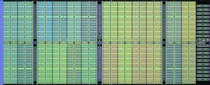 |
| 32nm SRAM with High-K/Metal Gate - world's smallest SRAM cell using High-K/Metal Gate ( < 0.15um2) |
Abstract:
Smaller, Faster More Power-Efficient* 32 Nanometer Semiconductors Span Low-Power Consumer Devices, High-Performance Computing
IBM Alliances Deliver Easier Path to Next Generation Semiconductor Products
ARMONK, NY | Posted on December 10th, 2007IBM (NYSE: IBM) and its joint development partners -- AMD, Chartered Semiconductor Manufacturing Ltd., Freescale, Infineon, and Samsung -- today announced an innovative approach to speed the implementation of a breakthrough material known as "high-k/metal gate" in next generation 32 nanometer (32nm) computer chips.
This new approach, an industry first based on what engineers call a "high-k gate-first" process, is designed to provide a simpler, less time consuming way for clients to migrate to high-k metal gate technology in order to secure benefits that include improved performance and reduced power consumption. Chips using the new technique will support a range of applications -- from low power computer microchips targeted at wireless and other consumer-oriented devices to high performance microprocessors for games and enterprise computing. This new approach to implementing high-k/metal gate will be available to IBM alliance members and their clients in the second half of 2009.**
On January 29, 2007, IBM and its research partners (including Sony and Toshiba) introduced the "high-k/metal gate" innovation as the basis for a long-sought improvement to the transistor -- the tiny on/off switch that serves as the basic building block of virtually all microchips made today. Using the high-k/metal gate material in a critical portion of the transistor that controls its primary on/off switching function enabled the development of 32nm chip circuitry that is designed to be smaller, faster, and more power-efficient than previously thought possible.
Using high-k/metal gate IBM and its Alliance Partners have been able to successfully shrink the size of a chip by up to 50 percent as compared to the previous technology generation while improving a number of other performance specifications. For example, high-k metal gate chips save about 45 percent total power, an increasingly critical metric in all electronics applications. Together these improvements will help to increase functionality and performance with lower power consumption and improved battery life in mobile devices. For microprocessor applications, this innovation also enables up to 30 percent higher performance as documented in measurements performed by IBM and its Alliance Partners at IBM's East Fishkill, NY semiconductor manufacturing facility.
"IBM's alliances have demonstrated the 'high-k gate-first' approach in a manufacturing environment, an achievement that provides clients with a simple, scalable pathway to incorporating the high k material innovation in semiconductor development without introducing additional design complexity," said Gary Patton, vice president, IBM's Semiconductor Research and Development Center on behalf of IBM's technology alliances. "This industry leading development comes from leveraging the collective engineering talent and breadth of market experience across the six Alliance Partner companies, as well as world-class R&D facilities such as UAlbany NanoCollege's Albany NanoTech complex, in order to maintain an aggressive road map."
IBM and its Alliance Partners have developed low-power foundry Complementary Metal Oxide Semiconductor (CMOS) technology using the 'high-k gate-first' approach and have demonstrated the first 32nm ultra dense static random access memory (SRAM) in this low power technology with cell sizes below 0.15um2. SRAMs are a key building block of computer chip designs and an excellent indicator of the readiness of a technology. The unique characteristics of the high-k material reduces total chip power consumption by as much as a 45 percent compared to the previous generation, a critical technology factor for achieving longer battery life in hand held devices such as cell phones, pagers, and PDAs.
In addition, IBM and its Alliance Partners have incorporated the high-k innovation into a new generation of high performance Silicon-On-Insulator (SOI) technology at 32nm. The unique high-k material properties enable a transistor speed improvement of greater than 30 percent over the previous generation of high performance Silicon-On-Insulator (SOI) technology. The SRAM demonstrated in this new generation of high performance technology functions at a lower voltage -- an improvement that reduces the energy consumption for microprocessor applications. The use of SOI provides a significant performance and power benefit, which, in combination with the high-k/metal gate advancement, will help the technology deliver energy efficient chips used in applications such as games, personal computers, and high end computing systems.
Today's announcement marks the latest development achievement from this alliance of semiconductor manufacturing, development and technology companies that collaborate to address the product design and advanced process development challenges central to producing a smaller, faster, more cost efficient generation of semiconductors.
* As documented in measurements performed by IBM and its Alliance Partners at IBM's East Fishkill, NY semiconductor manufacturing facility.
** All future dates and specifications are estimations only; subject to change without notice.
Note to Editors: A video is available in the IBM Press Room at http://www.ibm.com/press/us/en/pressrelease/22858.wss . A broadcast-quality version of the video can be downloaded by registered journalists at http://www.thenewsmarket.com/ibm .
####
For more information, please click here
Contacts:
AMD Contact:
Gary Silcott
AMD Public Relations
512-602-1480
Chartered Contact:
Tiffany Sparks
Media Relations
408-941-1185
Freescale Contact:
Andy North
Media Relations
512-996-4418
IBM Contact:
Bruce McConnel
IBM Media Relations
203-739-5462
Infineon Contact:
Reiner Schoenrock
Media Relations
Infineon Technologies AG
Phone +49 89 234 295 93
Fax +49 89 234 955 54 70
Mobile +49 160 530 4133
Samsung Contact:
Lisa Warren-Plungy
SSI Media Relations
408-544-5377
Copyright © Marketwire
If you have a comment, please Contact us.Issuers of news releases, not 7th Wave, Inc. or Nanotechnology Now, are solely responsible for the accuracy of the content.
Bookmark:


| Related News Press |
Chip Technology
![]() Discovery points path to flash-like memory for storing qubits: Rice find could hasten development of nonvolatile quantum memory April 5th, 2024
Discovery points path to flash-like memory for storing qubits: Rice find could hasten development of nonvolatile quantum memory April 5th, 2024
![]() Utilizing palladium for addressing contact issues of buried oxide thin film transistors April 5th, 2024
Utilizing palladium for addressing contact issues of buried oxide thin film transistors April 5th, 2024
![]() HKUST researchers develop new integration technique for efficient coupling of III-V and silicon February 16th, 2024
HKUST researchers develop new integration technique for efficient coupling of III-V and silicon February 16th, 2024
Announcements
![]() NRL charters Navy�s quantum inertial navigation path to reduce drift April 5th, 2024
NRL charters Navy�s quantum inertial navigation path to reduce drift April 5th, 2024
![]() Discovery points path to flash-like memory for storing qubits: Rice find could hasten development of nonvolatile quantum memory April 5th, 2024
Discovery points path to flash-like memory for storing qubits: Rice find could hasten development of nonvolatile quantum memory April 5th, 2024
Alliances/Trade associations/Partnerships/Distributorships
![]() Chicago Quantum Exchange welcomes six new partners highlighting quantum technology solutions, from Chicago and beyond September 23rd, 2022
Chicago Quantum Exchange welcomes six new partners highlighting quantum technology solutions, from Chicago and beyond September 23rd, 2022
![]() University of Illinois Chicago joins Brookhaven Lab's Quantum Center June 10th, 2022
University of Illinois Chicago joins Brookhaven Lab's Quantum Center June 10th, 2022
|
|
||
|
|
||
| The latest news from around the world, FREE | ||
|
|
||
|
|
||
| Premium Products | ||
|
|
||
|
Only the news you want to read!
Learn More |
||
|
|
||
|
Full-service, expert consulting
Learn More |
||
|
|
||