Home > Press > "Nature-Made" Computers Clark School Engineers Teach Nature to "Grow" High-Tech Components
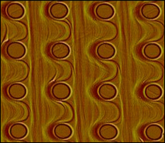 |
| Template self-organization--cylindrical pits on a silicon surface. |
Abstract:
Computers don't grow on trees, but with a little prodding from engineers, nature can produce computer components.
"Nature-Made" Computers Clark School Engineers Teach Nature to "Grow" High-Tech Components
COLLEGE PARK, MD | Posted on October 30th, 2007At the University of Maryland's A. James Clark School of Engineering, Ray Phaneuf, associate professor of materials science and engineering, has developed a template nature can follow to produce "self-assembling" structures. The template causes atoms to be arranged in a defined pattern that can serve a variety of purposes�a semiconductor in a laptop, a component in a cell phone or a sensor in a wearable device.
The idea of self-assembly in nature has long been known�crystallization is one such process; the formation of shells into spirals is another. However, researchers have been limited to the designs that nature already knows how to make. Phaneuf's work introduces a man-made template that nature then follows, addressing a number of manufacturing difficulties.
Patterned silicon surfaces."While we understand how to make working nanoscale devices, making things out of a countable number of atoms takes a long time," Phaneuf said. "Industry needs to be able to mass-produce them on a practical time scale."
The template process can be used by device manufacturers to mass-produce tiny components rapidly and efficiently, reduce costs, shrink device sizes, and improve devices' functionality in ways previously not possible.
"The same template can be used thousands of times," Phaneuf said. "This results in enormous savings."
Phaneuf says his work is one step in a "cocktail" approach to computer assembly�an engineer's dream in which one could "mix-up" a computer the same way one mixes a drink.
"Imagine you shake up a cocktail and spill it onto a table," Phaneuf said. "The liquid will collect in pools in a manner designated by nature.
"Now imagine that first you coated the table with wax and scraped a pattern into it. Now when you spill the liquid onto the table, it collects in the pattern you scraped into the wax�it assumes the form you want it to take. When we apply this idea to manufacturing nanoscale computer components, collections of atoms become ordered, accessible, controllable and reproducible�characteristics crucial to their use in high-tech devices."
These devices could include those used in the growing field of quantum computing, which is believed to hold promise for carrying out exceptionally difficult mathematical processes, Phaneuf said. An application of the templates might be self-assembly of coupled quantum dots to form "qubits," the building blocks of quantum computers. According to Phaneuf, templating could be used to make the manufacture of this highly complicated system more feasible: "Addressing individual qubits might be done optically, to get around the problem of trying to wire them all up."
Phaneuf's work focuses on silicon and gallium arsenide components. Silicon is the prevalent material for components in computers while gallium arsenide is used more often in cell phones.
The templates are created using photolithography (a process akin to photography, in which the template is chemically developed after being exposed to light) and etching, or by "nanoscraping," in which an atomic force microscope is used to selectively scrape the pattern into the template.
####
About A. James Clark School of Engineering
The Clark School of Engineering, situated on the rolling, 1,500-acre University of Maryland campus in College Park, Md., is one of the premier engineering schools in the U.S.
The Clark School's graduate programs are collectively the fastest rising in the nation. In U.S. News & World Report's annual rating of graduate programs, the school is 15th among public and private programs nationally, 9th among public programs nationally and first among public programs in the mid-Atlantic region. The School offers 13 graduate programs and 12 undergraduate programs, including degree and certification programs tailored for working professionals.
The school is home to one of the most vibrant research programs in the country. With major emphasis in key areas such as communications and networking, nanotechnology, bioengineering, reliability engineering, project management, intelligent transportation systems and space robotics, as well as electronic packaging and smart small systems and materials, the Clark School is leading the way toward the next generations of engineering advances.
Visit the Clark School homepage at http://www.eng.umd.edu .
For more information, please click here
Contacts:
Missy Corley
(301) 405-6501
Lee Tune
301-405-4679
Copyright © A. James Clark School of Engineering
If you have a comment, please Contact us.Issuers of news releases, not 7th Wave, Inc. or Nanotechnology Now, are solely responsible for the accuracy of the content.
Bookmark:


| Related Links |
![]() "Templating for Directed Self Assembly"
"Templating for Directed Self Assembly"
| Related News Press |
Chip Technology
![]() Discovery points path to flash-like memory for storing qubits: Rice find could hasten development of nonvolatile quantum memory April 5th, 2024
Discovery points path to flash-like memory for storing qubits: Rice find could hasten development of nonvolatile quantum memory April 5th, 2024
![]() Utilizing palladium for addressing contact issues of buried oxide thin film transistors April 5th, 2024
Utilizing palladium for addressing contact issues of buried oxide thin film transistors April 5th, 2024
![]() HKUST researchers develop new integration technique for efficient coupling of III-V and silicon February 16th, 2024
HKUST researchers develop new integration technique for efficient coupling of III-V and silicon February 16th, 2024
Self Assembly
![]() Liquid crystal templated chiral nanomaterials October 14th, 2022
Liquid crystal templated chiral nanomaterials October 14th, 2022
![]() Nanoclusters self-organize into centimeter-scale hierarchical assemblies April 22nd, 2022
Nanoclusters self-organize into centimeter-scale hierarchical assemblies April 22nd, 2022
![]() Atom by atom: building precise smaller nanoparticles with templates March 4th, 2022
Atom by atom: building precise smaller nanoparticles with templates March 4th, 2022
![]() Nanostructures get complex with electron equivalents: Nanoparticles of two different sizes break away from symmetrical designs January 14th, 2022
Nanostructures get complex with electron equivalents: Nanoparticles of two different sizes break away from symmetrical designs January 14th, 2022
Quantum Computing
![]() Simulating magnetization in a Heisenberg quantum spin chain April 5th, 2024
Simulating magnetization in a Heisenberg quantum spin chain April 5th, 2024
![]() Discovery points path to flash-like memory for storing qubits: Rice find could hasten development of nonvolatile quantum memory April 5th, 2024
Discovery points path to flash-like memory for storing qubits: Rice find could hasten development of nonvolatile quantum memory April 5th, 2024
![]() With VECSELs towards the quantum internet Fraunhofer: IAF achieves record output power with VECSEL for quantum frequency converters April 5th, 2024
With VECSELs towards the quantum internet Fraunhofer: IAF achieves record output power with VECSEL for quantum frequency converters April 5th, 2024
![]() Chemical reactions can scramble quantum information as well as black holes April 5th, 2024
Chemical reactions can scramble quantum information as well as black holes April 5th, 2024
Discoveries
![]() Chemical reactions can scramble quantum information as well as black holes April 5th, 2024
Chemical reactions can scramble quantum information as well as black holes April 5th, 2024
![]() New micromaterial releases nanoparticles that selectively destroy cancer cells April 5th, 2024
New micromaterial releases nanoparticles that selectively destroy cancer cells April 5th, 2024
![]() Utilizing palladium for addressing contact issues of buried oxide thin film transistors April 5th, 2024
Utilizing palladium for addressing contact issues of buried oxide thin film transistors April 5th, 2024
Announcements
![]() NRL charters Navy�s quantum inertial navigation path to reduce drift April 5th, 2024
NRL charters Navy�s quantum inertial navigation path to reduce drift April 5th, 2024
![]() Discovery points path to flash-like memory for storing qubits: Rice find could hasten development of nonvolatile quantum memory April 5th, 2024
Discovery points path to flash-like memory for storing qubits: Rice find could hasten development of nonvolatile quantum memory April 5th, 2024
|
|
||
|
|
||
| The latest news from around the world, FREE | ||
|
|
||
|
|
||
| Premium Products | ||
|
|
||
|
Only the news you want to read!
Learn More |
||
|
|
||
|
Full-service, expert consulting
Learn More |
||
|
|
||