Home > Press > Harvard University’s Center for Nanoscale Systems Selects Imaging and Analysis Instruments from Carl Zeiss SMT
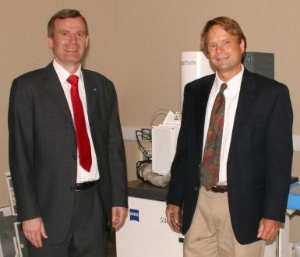 |
| Frank Averdung (left), President and General Manager of Carl Zeiss SMT Inc. hands over the first of a total of eight advanced microscope systems to Eric Martin, technical director at Harvard's CNS. (Photo: Business Wire) |
Abstract:
Carl Zeiss SMT, a leading global provider of electron- and ion-beam imaging and analysis equipment, today announced that Harvard University's Faculty for Arts and Sciences (FAS) has selected a number of its most advanced instruments for use at the FAS Center for Nanoscale Systems (CNS). CNS is a shared-use, core laboratory facility supporting a diverse community of investigators performing innovative nanoscale research.
Harvard University’s Center for Nanoscale Systems Selects Imaging and Analysis Instruments from Carl Zeiss SMT
PEABODY, MA | Posted on October 1st, 2007 The international researchers at Harvard CNS will have at their fingertips a total of eight of the most advanced ZEISS scanning- and transmission-electron microscopes, focused-ion-beam analytical systems, and one of the world's first helium ion microscopes. This suite of cutting-edge imaging and analytical instruments will enable unparalleled, multidisciplinary research and development at the frontiers of nanotechnology.
Dr. Dirk Stenkamp, member of the Carl Zeiss SMT AG executive board, described this collaboration as "the perfect match of research and technology excellence." He added, "It is a great honour for us, and a tribute to the superior capabilities of our instruments, that Harvard has selected Carl Zeiss SMT as its long-term strategic partner for CNS."
Eric Martin, the CNS Technical Director, says "our Center supports the imaging needs of hundreds of users each year and our selection process focused on technical excellence. Also critical for us is to have a partner with deep corporate commitment to the excellence of our facility and the success of our operational goals. We found both the technical and the partnership values in Carl Zeiss SMT."
The ZEISS systems included in the Harvard CNS order are:
* Two corrected/monochromated LIBRA® 200 Energy Filtering TEMs
* Two NVision 40 CrossBeam Focused Ion Beam (FIB) workstations
* One ULTRA 55 Gemini Column, Field Emission Scanning Electron Microscope (FE-SEM)
* One SUPRA® 55VP Gemini Column FE-SEM
* One EVO® 50EP Extended Pressure Analytical SEM
In addition, Harvard CNS will possess the latest and most revolutionary microscopy technology available—the ZEISS Orion™ helium ion microscope. This new breed of microscope is expected to provide images with never-before-seen, ultra-high spatial resolution and material contrast at a substantially extended depth of focus.
Frank Averdung, President and General Manager of Carl Zeiss SMT Inc. said, "With our North American headquarters located in Peabody, Massachusetts, we are now better positioned than ever to provide mutually beneficial support relationships with respect to application development and service quality to our customers in this part of the world."
CNS was created in 1999 to assist and support the community of Harvard University researchers and collaborators. The inclusion of CNS in the National Nanotechnology Infrastructure Network (NNIN) in 2004 expanded that function to include members of the larger research community, both local and national, academic and non-academic who conduct research regarding any aspect of the large and growing field of nanoscale science. In 2007 CNS moved into the newly opened Laboratory for Integrated Science and Engineering (LISE) which includes specialized facilities for the Center's three service areas: imaging, nanofabrication, and material characterization and synthesis.
####
About Carl Zeiss SMT
Carl Zeiss SMT utilizes its globally leading know-how in light, electron and ion-optical technologies to offer its customers in the manufacturing industry and R&D a broad portfolio of products, services and application solutions. The market-leading systems and solutions from Carl Zeiss SMT are used in mutually strengthening fields of application in nanotechnology such as semiconductor technology, materials research and the life sciences. The global customer community is constantly growing.
As the innovation leader for lithography optics, as well as optical and particle-beam based inspection, analysis and measuring systems, Carl Zeiss SMT opens up new avenues for its customers in industrial manufacturing environments, quality assurance and industrial and university R&D. Together with its subsidiaries in Germany, England, France and the USA, the international group of companies has approximately 2,400 employees.
In fiscal year 2005/06, Carl Zeiss SMT AG generated revenues of over EUR 860 million. Carl Zeiss SMT AG is a wholly owned subsidiary of Carl Zeiss AG.
For more information, please click here
Contacts:
Carl Zeiss SMT AG, Germany
Markus Wiederspahn
+49 7364 20-21 94
Public Relations
Copyright © Business Wire 2007
If you have a comment, please Contact us.Issuers of news releases, not 7th Wave, Inc. or Nanotechnology Now, are solely responsible for the accuracy of the content.
Bookmark:


| Related News Press |
Announcements
![]() NRL charters Navy’s quantum inertial navigation path to reduce drift April 5th, 2024
NRL charters Navy’s quantum inertial navigation path to reduce drift April 5th, 2024
![]() Discovery points path to flash-like memory for storing qubits: Rice find could hasten development of nonvolatile quantum memory April 5th, 2024
Discovery points path to flash-like memory for storing qubits: Rice find could hasten development of nonvolatile quantum memory April 5th, 2024
Tools
![]() Ferroelectrically modulate the Fermi level of graphene oxide to enhance SERS response November 3rd, 2023
Ferroelectrically modulate the Fermi level of graphene oxide to enhance SERS response November 3rd, 2023
![]() The USTC realizes In situ electron paramagnetic resonance spectroscopy using single nanodiamond sensors November 3rd, 2023
The USTC realizes In situ electron paramagnetic resonance spectroscopy using single nanodiamond sensors November 3rd, 2023
New-Contracts/Sales/Customers
![]() Bruker Light-Sheet Microscopes at Major Comprehensive Cancer Center: New Advanced Imaging Center Powered by Two MuVi and LCS SPIM Microscopes March 25th, 2021
Bruker Light-Sheet Microscopes at Major Comprehensive Cancer Center: New Advanced Imaging Center Powered by Two MuVi and LCS SPIM Microscopes March 25th, 2021
![]() Arrowhead Pharmaceuticals Announces Closing of Agreement with Takeda November 27th, 2020
Arrowhead Pharmaceuticals Announces Closing of Agreement with Takeda November 27th, 2020
![]() Veeco Announces Aledia Order of 300mm MOCVD Equipment for microLED Displays: Propel™ Platform First 300mm System with EFEM Designed for Advanced Display Applications October 20th, 2020
Veeco Announces Aledia Order of 300mm MOCVD Equipment for microLED Displays: Propel™ Platform First 300mm System with EFEM Designed for Advanced Display Applications October 20th, 2020
![]() GREENWAVES TECHNOLOGIES Announces Next Generation GAP9 Hearables Platform Using GLOBALFOUNDRIES 22FDX Solution October 16th, 2020
GREENWAVES TECHNOLOGIES Announces Next Generation GAP9 Hearables Platform Using GLOBALFOUNDRIES 22FDX Solution October 16th, 2020
|
|
||
|
|
||
| The latest news from around the world, FREE | ||
|
|
||
|
|
||
| Premium Products | ||
|
|
||
|
Only the news you want to read!
Learn More |
||
|
|
||
|
Full-service, expert consulting
Learn More |
||
|
|
||