Home > Press > Nanotube forests grown on silicon chips for future computers, electronics
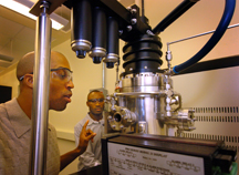 |
| Mechanical engineering doctoral student Baratunde A. Cola, from left, looks through a view port in a plasma-enhanced chemical vapor deposition instrument while postdoctoral research fellow Placidus Amama adjusts settings. The two engineers recently have shown how to grow forests of tiny cylinders called carbon nanotubes onto the surfaces of computer chips to enhance the flow of heat at a critical point where the chips connect to cooling devices called heat sinks. The carpetlike growth of nanotubes has been shown to outperform conventional "thermal interface materials." The research is based at the Birck Nanotechnology Center in Discovery Park at Purdue. (Purdue News Service photo/David Umberger) |
Abstract:
Engineers have shown how to grow forests of tiny cylinders called carbon nanotubes onto the surfaces of computer chips to enhance the flow of heat at a critical point where the chips connect to cooling devices called heat sinks.
Nanotube forests grown on silicon chips for future computers, electronics
WEST LAFAYETTE, IN | Posted on October 1st, 2007The carpetlike growth of nanotubes has been shown to outperform conventional "thermal interface materials." Like those materials, the nanotube layer does not require elaborate clean-room environments, representing a possible low-cost manufacturing approach to keep future chips from overheating and reduce the size of cooling systems, said Placidus B. Amama, a postdoctoral research associate at the Birck Nanotechnology Center in Purdue's Discovery Park.
Researchers are trying to develop new types of thermal interface materials that conduct heat more efficiently than conventional materials, improving overall performance and helping to meet cooling needs of future chips that will produce more heat than current microprocessors. The materials, which are sandwiched between silicon chips and the metal heat sinks, fill gaps and irregularities between the chip and metal surfaces to enhance heat flow between the two.
The method developed by the Purdue researchers enables them to create a nanotube interface that conforms to a heat sink's uneven surface, conducting heat with less resistance than comparable interface materials currently in use by industry, said doctoral student Baratunde A. Cola.
Findings were detailed in a research paper that appeared in September's issue of the journal Nanotechnology. The paper was written by Amama; Cola; Timothy D. Sands, director of the Birck Nanotechnology Center and the Basil S. Turner Professor of Materials Engineering and Electrical and Computer Engineering; and Xianfan Xu and Timothy S. Fisher, both professors of mechanical engineering.
Better thermal interface materials are needed either to test computer chips in manufacturing or to keep chips cooler during operation in commercial products.
"In a personal computer, laptop and portable electronics, the better your thermal interface material, the smaller the heat sink and overall chip-cooling systems have to be," Cola said.
Heat sinks are structures that usually contain an array of fins to increase surface contact with the air and improve heat dissipation, and a fan often also is used to blow air over the devices to cool chips.
Conventional thermal interface materials include greases, waxes and a foil made of a metal called indium. All of these materials, however, have drawbacks. The greases don't last many cycles of repeatedly testing chips on the assembly line. The indium foil doesn't make good enough contact for optimum heat transfer, Fisher said.
The Purdue researchers created templates from branching molecules called dendrimers, forming these templates on a silicon surface. Then, metal catalyst particles that are needed to grow the nanotubes were deposited inside cavities between the dendrimer branches. Heat was then applied to the silicon chip, burning away the polymer and leaving behind only the metal catalyst particles.
The engineers then placed the catalyst particle-laden silicon inside a chamber and exposed it to methane gas. Microwave energy was applied to break down the methane, which contains carbon. The catalyst particles prompted the nanotubes to assemble from carbon originating in the methane, and the tubes then grew vertically from the surface of the silicon chip.
"The dendrimer is a vehicle to deliver the cargo of catalyst particles, making it possible for us to seed the carbon nanotube growth right on the substrate," Amama said. "We are able to control the particle size - what ultimately determines the diameters of the tubes - and we also have control over the density, or the thickness of this forest of nanotubes. The density, quality and diameter are key parameters in controlling the heat-transfer properties."
The catalyst particles are made of "transition metals," such as iron, cobalt, nickel or palladium. Because the catalyst particles are about 10 nanometers in diameter, they allow the formation of tubes of similar diameter.
The branching dendrites are tipped with molecules called amines, which act as handles to stick to the silicon surface.
"This is important because for heat-transfer applications, you want the nanotubes to be well-anchored," Amama said.
Researchers usually produce carbon nanotubes separately and then attach them to the silicon chips or mix them with a polymer and then apply them as a paste.
"Our direct growth approach, however, addresses the critical heat-flow path, which is between the chip surface and the nanotubes themselves," Fisher said. "Without this direct connection, the thermal performance suffers greatly."
Because the dendrimers have a uniform composition and structure, the researchers were able to control the distribution and density of catalyst particles.
The research team also has been able to control the number of "defect sites" in the lattice of carbon atoms making up the tubes, creating tubes that are more flexible. This increased flexibility causes the nanotube forests to conform to the surface of the heat sink, making for better contact and improved heat conduction.
"The tubes bend like toothbrush bristles, and they stick into the gaps and make a lot of real contact," Cola said.
The carbon nanotubes were grown using a technique called microwave plasma chemical vapor deposition, a relatively inexpensive method for manufacturing a thermal-interface material made of carbon nanotubes, Fisher said.
"The plasma deposition approach allows us great flexibility in controlling the growth environment and has enabled us to grow carbon nanotube arrays over a broad range of substrate temperatures," Fisher said.
The research has been funded by NASA through the Institute for Nanoelectronics and Computing, based at Purdue's Discovery Park. Cola also received support through a fellowship from Intel Corp. and Purdue.
####
About Purdue University
Founded in 1869 and named after benefactor John Purdue, Purdue University began its journey with six instructors, 39 students and a mission to provide agriculture and mechanic arts education.
For more information, please click here
Contacts:
Writer: Emil Venere, (765) 494-4709,
Sources: Timothy Fisher, (765) 494-5627,
Timothy Sands, (765) 496-6105,
Placidus B. Amama, (765) 496-7407,
Baratunde A. Cola, (765) 496-8339,
Purdue News Service: (765) 494-2096;
Copyright © Purdue University
If you have a comment, please Contact us.Issuers of news releases, not 7th Wave, Inc. or Nanotechnology Now, are solely responsible for the accuracy of the content.
Bookmark:


| Related News Press |
Chip Technology
![]() Discovery points path to flash-like memory for storing qubits: Rice find could hasten development of nonvolatile quantum memory April 5th, 2024
Discovery points path to flash-like memory for storing qubits: Rice find could hasten development of nonvolatile quantum memory April 5th, 2024
![]() Utilizing palladium for addressing contact issues of buried oxide thin film transistors April 5th, 2024
Utilizing palladium for addressing contact issues of buried oxide thin film transistors April 5th, 2024
![]() HKUST researchers develop new integration technique for efficient coupling of III-V and silicon February 16th, 2024
HKUST researchers develop new integration technique for efficient coupling of III-V and silicon February 16th, 2024
Nanotubes/Buckyballs/Fullerenes/Nanorods/Nanostrings
![]() Tests find no free-standing nanotubes released from tire tread wear September 8th, 2023
Tests find no free-standing nanotubes released from tire tread wear September 8th, 2023
![]() Detection of bacteria and viruses with fluorescent nanotubes July 21st, 2023
Detection of bacteria and viruses with fluorescent nanotubes July 21st, 2023
Nanoelectronics
![]() Interdisciplinary: Rice team tackles the future of semiconductors Multiferroics could be the key to ultralow-energy computing October 6th, 2023
Interdisciplinary: Rice team tackles the future of semiconductors Multiferroics could be the key to ultralow-energy computing October 6th, 2023
![]() Key element for a scalable quantum computer: Physicists from Forschungszentrum J�lich and RWTH Aachen University demonstrate electron transport on a quantum chip September 23rd, 2022
Key element for a scalable quantum computer: Physicists from Forschungszentrum J�lich and RWTH Aachen University demonstrate electron transport on a quantum chip September 23rd, 2022
![]() Reduced power consumption in semiconductor devices September 23rd, 2022
Reduced power consumption in semiconductor devices September 23rd, 2022
![]() Atomic level deposition to extend Moore�s law and beyond July 15th, 2022
Atomic level deposition to extend Moore�s law and beyond July 15th, 2022
Discoveries
![]() Chemical reactions can scramble quantum information as well as black holes April 5th, 2024
Chemical reactions can scramble quantum information as well as black holes April 5th, 2024
![]() New micromaterial releases nanoparticles that selectively destroy cancer cells April 5th, 2024
New micromaterial releases nanoparticles that selectively destroy cancer cells April 5th, 2024
![]() Utilizing palladium for addressing contact issues of buried oxide thin film transistors April 5th, 2024
Utilizing palladium for addressing contact issues of buried oxide thin film transistors April 5th, 2024
Announcements
![]() NRL charters Navy�s quantum inertial navigation path to reduce drift April 5th, 2024
NRL charters Navy�s quantum inertial navigation path to reduce drift April 5th, 2024
![]() Discovery points path to flash-like memory for storing qubits: Rice find could hasten development of nonvolatile quantum memory April 5th, 2024
Discovery points path to flash-like memory for storing qubits: Rice find could hasten development of nonvolatile quantum memory April 5th, 2024
|
|
||
|
|
||
| The latest news from around the world, FREE | ||
|
|
||
|
|
||
| Premium Products | ||
|
|
||
|
Only the news you want to read!
Learn More |
||
|
|
||
|
Full-service, expert consulting
Learn More |
||
|
|
||