Home > Press > NANOIDENT CTO to Speak About Printed Sensor Applications at the Organic Electronics Conference 2007
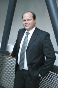 |
| Franz Padinger, CTO and Co-Founder of NANOIDENT Technologies AG (Photo: Business Wire) |
Abstract:
Printed Semiconductor Technology Turns "Chip in a Lab" Into "Lab on a Chip"
NANOIDENT CTO to Speak About Printed Sensor Applications at the Organic Electronics Conference 2007
LINZ, Austria | Posted on September 19th, 2007DI Franz Padinger, CTO for NANOIDENT Technologies AG, will speak about "Semiconductor 2.0: Products and Perspectives" at the Organic Electronics Conference & Exhibition 2007. He will explain how printed semiconductor technology has taken mobile analytics and diagnostics completely out of the lab, enabling the development of cost-effective, highly sensitive mobile testing solutions for the life sciences market.
NANOIDENT Technologies AG is the technology leader in the development and manufacture of printed semiconductor-based sensor solutions. One of its market-focused subsidiaries, BIOIDENT Technologies Inc., leverages this core technology to deliver lab-on-a-chip systems for mobile analysis and diagnosis, enabling cost-effective real-time detection of multiple chemical and biological parameters. BIOIDENT offers complete solutions for medical, environmental and chemical/biological testing applications.
WHO:
DI Franz Padinger, CTO, NANOIDENT Technologies AG
Mr. Padinger, a world-renowned scientist in the field of organic
semiconductor photophysics, photochemistry and photovoltaics,
developed the world's first plastic solar cell and is responsible for
NANOIDENT's R&D activities. Prior to co-founding NANOIDENT, he served
for two years as the CTO of Konarka Austria, where he worked with Dr.
Alan Heeger, Nobel Laureate and inventor of organic semiconductors.
WHEN:
Tuesday, September 25, 2007
2:30 p.m. - 3:00 p.m. CET
WHERE:
Organic Electronics Conference & Exhibition 2007
Sheraton Frankfurt Hotel and Towers, Frankfurt, Germany
The 5th annual Organic Electronics Conference & Exhibition is hosted
by cintelliq, a leading analyst for the organic electronics industry,
and by the Organic Electronics Association (OE-A), the key industry
association for organic electronics. The conference covers a broad
range of topics, from applications to materials, equipment and process
technology, and draws scientists, engineers, manufacturers and
investors in organic semiconductor technologies and organic
electronics.
WHY:
NANOIDENT's unique expertise with printed optoelectronics allows a
photodetector to be printed directly onto the lab-on-a-chip, greatly
increasing system sensitivity while significantly decreasing system
cost and complexity. As a result, affordable mobile analytics and
diagnostics are available for a wide range of applications, from
medical diagnosis to environmental testing to the detection of
chemical and biological agents, providing real-time, point-of-use
results to enable faster response to disease or contamination.
####
About NANOIDENT Technologies AG
NANOIDENT is the world leader in the development and manufacture of printed semiconductor based optoelectronic sensors. The company�s core technology merges the latest breakthroughs in materials science and nanotechnology with modern printing techniques to create a new class of semiconductor devices. The revolutionary SEMICONDUCTOR 2.0� Platform is the basis of the world�s first commercial printed photonic sensors, enabling a whole new generation of applications in the industrial, biometric and life science markets.
NANOIDENT�s high-speed, environmentally friendly manufacturing process utilizes liquid nanomaterials and additive production techniques. These liquids are used to print electronic circuits on a wide variety of surfaces, producing products in mere hours for prototype as well as high volume applications. The company�s printed semiconductor devices can be bendable, disposable, light, ultrathin and large area. They have application specific spectral and electronic properties, and can contain light sources and light detectors as well as electronic circuits. These unique characteristics enable cost effective, custom designed devices for applications such as industrial, chemical, biological, biometric and X-ray sensors, and smart packaging.
Privately held, the company is headquartered in Linz, Austria, with subsidiaries in Menlo Park, California; Nuremberg, Germany; and Grenoble, France.
To schedule a meeting with Mr. Padinger, or for more information about NANOIDENT, please contact 415-512-0770 or email .
For more information, please click here
Contacts:
NANOIDENT Technologies AG
Ulrike Kaiser, +43 732 9024 0
Fax: +43 732 9044 5
or
Schwartz Communications, Inc.
Marisa Dulyachinda or Britt Gottlieb, +1-415-512-0770
Copyright © Business Wire 2007
If you have a comment, please Contact us.Issuers of news releases, not 7th Wave, Inc. or Nanotechnology Now, are solely responsible for the accuracy of the content.
Bookmark:


| Related News Press |
Sensors
Announcements
![]() NRL charters Navy�s quantum inertial navigation path to reduce drift April 5th, 2024
NRL charters Navy�s quantum inertial navigation path to reduce drift April 5th, 2024
![]() Discovery points path to flash-like memory for storing qubits: Rice find could hasten development of nonvolatile quantum memory April 5th, 2024
Discovery points path to flash-like memory for storing qubits: Rice find could hasten development of nonvolatile quantum memory April 5th, 2024
Events/Classes
![]() Researchers demonstrate co-propagation of quantum and classical signals: Study shows that quantum encryption can be implemented in existing fiber networks January 20th, 2023
Researchers demonstrate co-propagation of quantum and classical signals: Study shows that quantum encryption can be implemented in existing fiber networks January 20th, 2023
Printing/Lithography/Inkjet/Inks/Bio-printing/Dyes
![]() Presenting: Ultrasound-based printing of 3D materials�potentially inside the body December 8th, 2023
Presenting: Ultrasound-based printing of 3D materials�potentially inside the body December 8th, 2023
![]() Simple ballpoint pen can write custom LEDs August 11th, 2023
Simple ballpoint pen can write custom LEDs August 11th, 2023
![]() Disposable electronics on a simple sheet of paper October 7th, 2022
Disposable electronics on a simple sheet of paper October 7th, 2022
|
|
||
|
|
||
| The latest news from around the world, FREE | ||
|
|
||
|
|
||
| Premium Products | ||
|
|
||
|
Only the news you want to read!
Learn More |
||
|
|
||
|
Full-service, expert consulting
Learn More |
||
|
|
||