Home > Press > NIST Team Develops Novel Method for Nanostructured Polymer Thin Films
 |
Abstract:
All researchers at the National Institute of Standards and Technology (NIST) wanted was a simple, quick method for making thin films of block copolymers or BCPs (chemically distinct polymers linked together) in order to have decent samples for taking measurements important to the microelectronics industry. What they got for their efforts, as detailed in the Sept. 12, 2007, Nano Letters,* was an unexpected bonus: a unique annealing process that may make practical the use of BCP thin films for patterning nanoscale features in next-generation microchips and data storage devices.
NIST Team Develops Novel Method for Nanostructured Polymer Thin Films
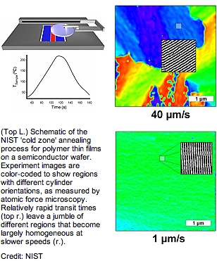
GAITHERSBURG, MD | Posted on September 14th, 2007BCP thin films have been highly desired by semiconductor manufacturers as patterns for laying down very fine features on microchips, such as arrays of tightly spaced, nanoscale lines. Annealing certain BCP films�a controlled heating process�causes one of the two polymer components to segregate into regular patterns of nanocylinder lines separated by distances as small as five nanometers or equally regular arrays of nanoscale dots. Chemically removing the other polymer leaves the pattern behind as a template for building structures on the microchip.
In traditional oven annealing the quality of the films is still insufficient even after days of annealing. A process called hot zone annealing�where the thin film moves at an extremely slow speed through a heated region that temporarily raises its temperature to a point just above that at which the cylinders become disordered�has previously been used for creating highly ordered BCP thin films with a minimum of defects but little orientation control. For some polymer combinations, the order-disorder transition temperature is so high that it is virtually impossible for manufacturers to heat them sufficiently without degradation occurring.
To eliminate the time and temperature restraints without losing the order yielded by hot zone annealing, the NIST researchers developed a "cold zone" annealing system where the polymers are completely processed well below their order-disorder transition temperature. Properly controlled, the lower-temperature processing not only works with BCPs for which hot-zone annealing is impractical, but, as the NIST experiments showed, also repeatedly produces a highly ordered thin film in a matter of minutes. NIST researchers also discovered that the alignment of the cylinders was controlled by the "cold zone" annealing conditions. Because it is simple, yields consistent product quality and has virtually no limitations on sample dimensions, the NIST method is being evaluated by microelectronic companies to fabricate highly ordered sub 30 nm features.
The next step, the NIST researchers say, is to better understand the fundamental processes that make the cold zone annealing system work so well and refine the measurements needed to evaluate its performance.
* B.C. Berry, A.W. Bosse, J.F. Douglas, R.L. Jones and A. Karim.Orientational order in block copolymer films zone annealed below the order-disorder transition temperature. Nano Letters, Vol. 7, No. 9, pp. 2789-2794, (Sept. 12, 2007).
####
About NST
From automated teller machines and atomic clocks to mammograms and semiconductors, innumerable products and services rely in some way on technology, measurement, and standards provided by the National Institute of Standards and Technology.
Founded in 1901, NIST is a non-regulatory federal agency within the U.S. Department of Commerce. NIST's mission is to promote U.S. innovation and industrial competitiveness by advancing measurement science, standards, and technology in ways that enhance economic security and improve our quality of life.
For more information, please click here
Contacts:
Michael E. Newman
(301) 975-3025
Copyright © NIST
If you have a comment, please Contact us.Issuers of news releases, not 7th Wave, Inc. or Nanotechnology Now, are solely responsible for the accuracy of the content.
Bookmark:


| Related News Press |
Chip Technology
![]() Discovery points path to flash-like memory for storing qubits: Rice find could hasten development of nonvolatile quantum memory April 5th, 2024
Discovery points path to flash-like memory for storing qubits: Rice find could hasten development of nonvolatile quantum memory April 5th, 2024
![]() Utilizing palladium for addressing contact issues of buried oxide thin film transistors April 5th, 2024
Utilizing palladium for addressing contact issues of buried oxide thin film transistors April 5th, 2024
![]() HKUST researchers develop new integration technique for efficient coupling of III-V and silicon February 16th, 2024
HKUST researchers develop new integration technique for efficient coupling of III-V and silicon February 16th, 2024
Memory Technology
![]() Utilizing palladium for addressing contact issues of buried oxide thin film transistors April 5th, 2024
Utilizing palladium for addressing contact issues of buried oxide thin film transistors April 5th, 2024
![]() Interdisciplinary: Rice team tackles the future of semiconductors Multiferroics could be the key to ultralow-energy computing October 6th, 2023
Interdisciplinary: Rice team tackles the future of semiconductors Multiferroics could be the key to ultralow-energy computing October 6th, 2023
![]() Researchers discover materials exhibiting huge magnetoresistance June 9th, 2023
Researchers discover materials exhibiting huge magnetoresistance June 9th, 2023
Discoveries
![]() Chemical reactions can scramble quantum information as well as black holes April 5th, 2024
Chemical reactions can scramble quantum information as well as black holes April 5th, 2024
![]() New micromaterial releases nanoparticles that selectively destroy cancer cells April 5th, 2024
New micromaterial releases nanoparticles that selectively destroy cancer cells April 5th, 2024
![]() Utilizing palladium for addressing contact issues of buried oxide thin film transistors April 5th, 2024
Utilizing palladium for addressing contact issues of buried oxide thin film transistors April 5th, 2024
Materials/Metamaterials/Magnetoresistance
![]() Nanoscale CL thermometry with lanthanide-doped heavy-metal oxide in TEM March 8th, 2024
Nanoscale CL thermometry with lanthanide-doped heavy-metal oxide in TEM March 8th, 2024
![]() Focused ion beam technology: A single tool for a wide range of applications January 12th, 2024
Focused ion beam technology: A single tool for a wide range of applications January 12th, 2024
Announcements
![]() NRL charters Navy�s quantum inertial navigation path to reduce drift April 5th, 2024
NRL charters Navy�s quantum inertial navigation path to reduce drift April 5th, 2024
![]() Discovery points path to flash-like memory for storing qubits: Rice find could hasten development of nonvolatile quantum memory April 5th, 2024
Discovery points path to flash-like memory for storing qubits: Rice find could hasten development of nonvolatile quantum memory April 5th, 2024
|
|
||
|
|
||
| The latest news from around the world, FREE | ||
|
|
||
|
|
||
| Premium Products | ||
|
|
||
|
Only the news you want to read!
Learn More |
||
|
|
||
|
Full-service, expert consulting
Learn More |
||
|
|
||