Home > Press > Harvard Researchers Select the ELIONIX 100kV Electron Beam Lithography System for Nanoscale Fabrication
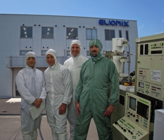 |
| The CNS 100kV System built at the Elionix NanoTech Center for delivery to the Harvard campus. |
Abstract:
SEMTech Solutions, Inc., announced that it will deliver an Elionix 100kV Electron Beam Lithography system to Harvard‚s FAS Center for Nanoscale Systems (CNS) in October.
Harvard Researchers Select the ELIONIX 100kV Electron Beam Lithography System for Nanoscale Fabrication
BILLERICA, MA | Posted on September 13th, 2007SEMTech Solutions, Inc., announced that it will deliver an Elionix 100kV Electron Beam Lithography system to Harvard's FAS Center for Nanoscale Systems (CNS) in October. The CNS at Harvard is an open, shared-use facility serving hundreds of researchers each year. It is part of the NSF's National Nanotechnology Infrastructure Network (NNIN). The Elionix ELS-7000 will be used by CNS users to fabricate nanoscale devices for advanced research projects.
"I am very pleased with the recent orders from Harvard and other major universities in the U.S.," states Seigo Honme, Elionix President. "After having established the highest market share for electron beam lithography systems in Japan and the Far East, I am confident that our teamwork with SEMTech Solutions in North America will find an increasing number of customers who will come to appreciate the high performance of Elionix systems."
Eric Martin, Technical Director for CNS says, "We were very impressed with the performance of the ELS-7000 system. We are also pleased with the commitment from the Elionix team to help us meet our Center's objectives for excellent technical service."
The Elionix ELS-7000 is an ultra high precision electron beam lithography system capable of generating patterns with a line width of less than 8nm. The system provides a stable 1.8nm electron beam using high beam currents at 100kV. Fine line patterns can be drawn using commercially available resists.
####
About SEMTech Solutions, Inc.
SEMTech Solutions is a leading North American sales and service representation company handling scientific instrumentation. In addition, we are also a leading supplier of refurbished SEMs and SEM services. With a growing customer base of over 100 companies, ranging from start-ups to Fortune 500 industries, we have the electron beam knowledge to meet any demand.
ELIONIX, Inc.
Elionix is a worldwide leading manufacturer of electron beam lithography systems, 3-D surface roughness measurement systems, and other pieces of equipment dedicated to nanotechnology. Located in Tokyo, Japan, Elionix is a privately held company that has spearheaded the development of advanced equipment for next generation technologies for over 30 years.
For more information, please click here
Contacts:
Gary Brake
Phone: 978-663-9822
Copyright © SEMTech Solutions, Inc.
If you have a comment, please Contact us.Issuers of news releases, not 7th Wave, Inc. or Nanotechnology Now, are solely responsible for the accuracy of the content.
Bookmark:


| Related News Press |
Academic/Education
![]() Rice University launches Rice Synthetic Biology Institute to improve lives January 12th, 2024
Rice University launches Rice Synthetic Biology Institute to improve lives January 12th, 2024
![]() Multi-institution, $4.6 million NSF grant to fund nanotechnology training September 9th, 2022
Multi-institution, $4.6 million NSF grant to fund nanotechnology training September 9th, 2022
Announcements
![]() NRL charters Navy’s quantum inertial navigation path to reduce drift April 5th, 2024
NRL charters Navy’s quantum inertial navigation path to reduce drift April 5th, 2024
![]() Discovery points path to flash-like memory for storing qubits: Rice find could hasten development of nonvolatile quantum memory April 5th, 2024
Discovery points path to flash-like memory for storing qubits: Rice find could hasten development of nonvolatile quantum memory April 5th, 2024
Tools
![]() Ferroelectrically modulate the Fermi level of graphene oxide to enhance SERS response November 3rd, 2023
Ferroelectrically modulate the Fermi level of graphene oxide to enhance SERS response November 3rd, 2023
![]() The USTC realizes In situ electron paramagnetic resonance spectroscopy using single nanodiamond sensors November 3rd, 2023
The USTC realizes In situ electron paramagnetic resonance spectroscopy using single nanodiamond sensors November 3rd, 2023
|
|
||
|
|
||
| The latest news from around the world, FREE | ||
|
|
||
|
|
||
| Premium Products | ||
|
|
||
|
Only the news you want to read!
Learn More |
||
|
|
||
|
Full-service, expert consulting
Learn More |
||
|
|
||