Home > Press > NANOIDENT developer to speak about the next generation of printed lab-on-a-chip devices at SPIE Europe Security & Defence 2007
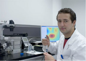 |
| NANOIDENT Life Sciences Developer DI Roland Pieler |
Abstract:
Printed photonics technology enables truly mobile analytics & diagnostics
NANOIDENT developer to speak about the next generation of printed lab-on-a-chip devices at SPIE Europe Security & Defence 2007
Linz, Austria | Posted on September 11th, 2007Roland Pieler, Developer for NANOIDENT Technologies AG's Life Sciences Division, will
present "Printed Photonics for Lab-on-Chip Applications" at SPIE Europe Security &
Defence 2007. Mr. Pieler will explain how printed photonics technology improves the
functionality of lab-on-a-chip systems, enabling true real-time, point-of-use diagnostics
and analytics.
NANOIDENT Technologies AG is the technology leader in the development and
manufacture of printed semiconductor-based sensor solutions. BIOIDENT Technologies
Inc., one of NANOIDENT's market-focused subsidiaries, leverages NANOIDENT's
technology to provide printed semiconductor-based photonic lab-on-a-chip solutions for
life sciences. BIOIDENT's PhotonicLab� platform received the 2007 Frost & Sullivan
Enabling Technology of the Year Award, and enables real-time, multi-parameter detection
and analysis capability for environmental testing, chemical and biological threat detection
and in-vitro diagnostics applications.
WHO:
DI Roland Pieler, Developer, NANOIDENT Life Sciences Division
Roland Pieler studied electrical and biomedical engineering at the University of
Technology Graz, Austria. After finishing his degree, he continued working at the Institute
of Genomics and Bioinformatics, Graz, in the field of Microarray Analysis and Software
Engineering. Soon he joined the Device Development division at the newly founded
�Center for Biomedical Nanotechnology" at UAR (Upper Austrian Research), Linz, Austria.
There, his main activities included software and hardware development for a
multipurpose fluorescence scanner. Mr. Pieler is well published, having authored
publications in professional journals in the field of Bioinformatics. As a member of
NANOIDENT's R&D team, he is responsible for prototype development, sensor layout and
software engineering issues.
WHEN:
Tuesday, September 18, 2007
3:10 p.m. - 3:30 p.m. CET
WHERE:
SPIE Europe Security & Defence 2007
Palazzo degli Affari, Florence, Italy
The 4th European Symposium on Optics/Photonics in Security & Defence is organized by
SPIE Europe. The conference will address both applications and underlying science in
advanced defense and security systems, as well as the challenges brought about by
network capabilities in military operations and the increasing need for urban
peacekeeping activities. With a European focus, this event attracts more than 400
attendees from government, academia and industry.
WHY:
NANOIDENT's printed semiconductor technology, combined with BIOIDENT's expertise in
microfluidics and chemical/biological testing, are changing the game in the mobile
analytics and diagnostics market. Medical, environmental and chemical/biological tests
no longer require bulky, expensive equipment; as a result, these highly sensitive tests can
be performed at lower cost, onsite in real-time, ensuring faster response to disease or
contamination.
####
About NANOIDENT Technologies AG
NANOIDENT is the world leader in the development and manufacture of printed
semiconductor based optoelectronic sensors. The company�s core technology merges
the latest breakthroughs in materials science and nanotechnology with modern printing techniques to create a new class of semiconductor devices. The revolutionary SEMICONDUCTOR 2.0� Platform is the basis of the world�s first commercial printed photonic sensors, enabling a whole new generation of applications in the industrial, biometric and life science markets.
NANOIDENT�s high speed, environmentally friendly manufacturing process utilizes liquid nanomaterials and additive production techniques. These liquids are used to print electronic circuits on a wide variety of surfaces, producing products in mere hours for prototype as well as high volume applications. The company�s printed semiconductor devices can be bendable, disposable, light, ultrathin and large area. They have application specific spectral and electronic properties, and can contain light sources and light detectors as well as electronic circuits. These unique characteristics enable cost effective, custom designed devices for applications such as industrial, chemical, biological, biometric and X-ray sensors, printed OLED displays for smart packaging and electronic signage.
Privately-held, the company is headquartered in Linz, Austria, with subsidiaries in Menlo Park, California; Nuremberg, Germany; and Grenoble, France.
For more information, please click here
Contacts:
NANOIDENT Technologies
Ulrike Kaiser
Untere Donaulaende 21� 25
A - 4020 Linz
Tel.: +43 732 9024 0
Fax: +43 732 9044 5
e-Mail:
AG Schwartz Communications, Inc.
Marisa Dulyachinda or Monica Miller
595 Market Street, Suite 2050
San Francisco, CA 94105, USA
Tel.: + 1 415 512 0770
e-Mail:
Copyright © NANOIDENT Technologies AG
If you have a comment, please Contact us.Issuers of news releases, not 7th Wave, Inc. or Nanotechnology Now, are solely responsible for the accuracy of the content.
Bookmark:


| Related News Press |
Announcements
![]() NRL charters Navy�s quantum inertial navigation path to reduce drift April 5th, 2024
NRL charters Navy�s quantum inertial navigation path to reduce drift April 5th, 2024
![]() Discovery points path to flash-like memory for storing qubits: Rice find could hasten development of nonvolatile quantum memory April 5th, 2024
Discovery points path to flash-like memory for storing qubits: Rice find could hasten development of nonvolatile quantum memory April 5th, 2024
Homeland Security
![]() The picture of health: Virginia Tech researchers enhance bioimaging and sensing with quantum photonics June 30th, 2023
The picture of health: Virginia Tech researchers enhance bioimaging and sensing with quantum photonics June 30th, 2023
![]() Sensors developed at URI can identify threats at the molecular level: More sensitive than a dog's nose and the sensors don't get tired May 21st, 2021
Sensors developed at URI can identify threats at the molecular level: More sensitive than a dog's nose and the sensors don't get tired May 21st, 2021
![]() Highly sensitive dopamine detector uses 2D materials August 7th, 2020
Highly sensitive dopamine detector uses 2D materials August 7th, 2020
Military
![]() NRL charters Navy�s quantum inertial navigation path to reduce drift April 5th, 2024
NRL charters Navy�s quantum inertial navigation path to reduce drift April 5th, 2024
![]() What heat can tell us about battery chemistry: using the Peltier effect to study lithium-ion cells March 8th, 2024
What heat can tell us about battery chemistry: using the Peltier effect to study lithium-ion cells March 8th, 2024
![]() New chip opens door to AI computing at light speed February 16th, 2024
New chip opens door to AI computing at light speed February 16th, 2024
Events/Classes
![]() Researchers demonstrate co-propagation of quantum and classical signals: Study shows that quantum encryption can be implemented in existing fiber networks January 20th, 2023
Researchers demonstrate co-propagation of quantum and classical signals: Study shows that quantum encryption can be implemented in existing fiber networks January 20th, 2023
|
|
||
|
|
||
| The latest news from around the world, FREE | ||
|
|
||
|
|
||
| Premium Products | ||
|
|
||
|
Only the news you want to read!
Learn More |
||
|
|
||
|
Full-service, expert consulting
Learn More |
||
|
|
||