Home > Press > Leading expertise in ALD and nanotechnology
 |
Abstract:
The annual Shareholders' Meeting of Picosun Oy has elected Prof. Jorma Routti, Prof. Lauri Niinistö, and Dr. Tuomo Suntola as new Board members. All the old members continue in the Board.
Leading expertise in ALD and nanotechnology
Helsinki, Finland | Posted on June 20th, 2007Professor, Ph.D Jorma Routti is one of the founders of Finnish venture capital and one of Europe's leading technology experts. Professor Routti is the Chairman of Creative Industries Management Ltd. and has managed Knowledge Economy Projects at World Bank since 2003. Professor Routti was Director General of Research at the European Commission from 1985 to 2000. His long career also includes heading the Finnish National Fund for Research and Development (SITRA), being the Dean of Helsinki University of Technology, and a visiting scientist at CERN, Geneva. At SITRA he made numerous private placements in Finnish and international technology companies, several of which were successfully floated. His numerous honors include a Fullbright Fellowship, an Eisenhower Exchange Fellowship, and Chevakier dans l'ordre des Palmes Acedemiques, France. He holds a Ph.D from UCLA Berkeley and several honorary doctorates.
Professor, Dr. Tech. Lauri Niinistö is one of the key persons in developing Atomic Layer Deposition processes and applications in Academia since late 1970s. He has more than 500 original publications and reviews on inorganic, analytical and materials chemistry, several textbooks (in Finnish), articles on the history of chemistry. His most recent research is focused on the preparation and characterization of thin films and overlayers for electronic, catalytic and sensor applications. He has acted as a visiting Professor at University of Florida in 1985 - 86, Technical University of Vienna in 1993 and at Budapest University of Technology and Economics in 2000. His career includes heading of several organizations and societies, such as Finnish Chemical Society, Federation of European Chemical Societies (FECS), FECS Working Party on Analytical Chemistry (since 1997: Division of Analytical Chemistry) and European Rare Earth Research Society (ERES). He is the editor or editorial board member of several Scientific Journals. His numerous recognitions and awards include Stanislao Cannizzaro Gold Medal of the Italian Chemical Society and FECS Award. He holds a Dr. Tech. from Helsinki University of Technology and two honorary doctorates.
Dr. Tech. Tuomo Suntola is the inventor of ALD method and Executive Advisor of Picosun Oy through Suntola Consulting Ltd. since the start of Picosun. Dr. Suntola introduced ALD with potential to electro-luminescent flat panel display application in 1974 - 1977. He was the initiator and the head of flat panel display division at Lohja Oy in 1977 - 1987 and the founder and Directing Manager of Microchemistry Ltd. in 1987 - 1997. Dr. Suntola has developed ALD for industrial production of electroluminescent flat panel displays and started the expansion of ALD technology to semiconductor applications and catalytic surface fabrication. Dr. Suntola was R&D Fellow at Neste Oy and Senior Scientific Advisor at Fortum Oyj 1998 - 2003. His current research has emphasis on sustainable energy future. Dr. Suntola is the author of numerous publications and patents regarding ALD, Thin Film Devices, Photovoltaics, renewable energy, climate change and fundamentals of Physics. His numerous honors and awards include The Finnish Engineering Achievement Award 1985 for Electroluminescent Display Technology and 2001 and European SEMI Award 2004, for the development of the ALD technology to semiconductor applications. Dr. Suntola is Knight 1st Class of the Order of the Lion of Finland and holds a Dr. Tech. from Helsinki University of Technology.
####
About Picosun Oy
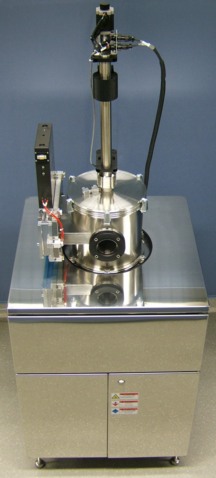
Picosun Oy, a Finnish company started in Espoo in 2003, develops and manufactures ALD reactors for nanotechnology applications. Atomic Layer Deposition (ALD) is a thin film deposition method that has been developed in Finland since 1974. ALD technology enables thin-film coating of nanosize structures and objects with a desired film thickness, conforming to the shapes of the surface precisely. ALD method has been applied successfully in manufacturing thin displays, microprocessors, mass memories, solar panels and catalytic materials.
For more information, please click here
Contacts:
Managing Director Juhana Kostamo
Picosun Oy
Tietotie 3, FI-02150 Espoo, Finland
Tel. +358 50 321 1955
Copyright © Picosun Oy
If you have a comment, please Contact us.Issuers of news releases, not 7th Wave, Inc. or Nanotechnology Now, are solely responsible for the accuracy of the content.
Bookmark:


| Related News Press |
Display technology/LEDs/SS Lighting/OLEDs
![]() Utilizing palladium for addressing contact issues of buried oxide thin film transistors April 5th, 2024
Utilizing palladium for addressing contact issues of buried oxide thin film transistors April 5th, 2024
![]() Light guide plate based on perovskite nanocomposites November 3rd, 2023
Light guide plate based on perovskite nanocomposites November 3rd, 2023
![]() Simple ballpoint pen can write custom LEDs August 11th, 2023
Simple ballpoint pen can write custom LEDs August 11th, 2023
![]() Novel design perovskite electrochemical cell for light-emission and light-detection May 12th, 2023
Novel design perovskite electrochemical cell for light-emission and light-detection May 12th, 2023
Chip Technology
![]() Discovery points path to flash-like memory for storing qubits: Rice find could hasten development of nonvolatile quantum memory April 5th, 2024
Discovery points path to flash-like memory for storing qubits: Rice find could hasten development of nonvolatile quantum memory April 5th, 2024
![]() Utilizing palladium for addressing contact issues of buried oxide thin film transistors April 5th, 2024
Utilizing palladium for addressing contact issues of buried oxide thin film transistors April 5th, 2024
![]() HKUST researchers develop new integration technique for efficient coupling of III-V and silicon February 16th, 2024
HKUST researchers develop new integration technique for efficient coupling of III-V and silicon February 16th, 2024
Materials/Metamaterials/Magnetoresistance
![]() Nanoscale CL thermometry with lanthanide-doped heavy-metal oxide in TEM March 8th, 2024
Nanoscale CL thermometry with lanthanide-doped heavy-metal oxide in TEM March 8th, 2024
![]() Focused ion beam technology: A single tool for a wide range of applications January 12th, 2024
Focused ion beam technology: A single tool for a wide range of applications January 12th, 2024
Announcements
![]() NRL charters Navy’s quantum inertial navigation path to reduce drift April 5th, 2024
NRL charters Navy’s quantum inertial navigation path to reduce drift April 5th, 2024
![]() Discovery points path to flash-like memory for storing qubits: Rice find could hasten development of nonvolatile quantum memory April 5th, 2024
Discovery points path to flash-like memory for storing qubits: Rice find could hasten development of nonvolatile quantum memory April 5th, 2024
Tools
![]() Ferroelectrically modulate the Fermi level of graphene oxide to enhance SERS response November 3rd, 2023
Ferroelectrically modulate the Fermi level of graphene oxide to enhance SERS response November 3rd, 2023
![]() The USTC realizes In situ electron paramagnetic resonance spectroscopy using single nanodiamond sensors November 3rd, 2023
The USTC realizes In situ electron paramagnetic resonance spectroscopy using single nanodiamond sensors November 3rd, 2023
Appointments/Promotions/New hires/Resignations/Deaths
![]() Leibniz Prize winner Professor Dr. Oliver G. Schmidt moves to Chemnitz University of Technology: President Professor Dr. Gerd Strohmeier refers to an 'absolute top transfer' September 10th, 2021
Leibniz Prize winner Professor Dr. Oliver G. Schmidt moves to Chemnitz University of Technology: President Professor Dr. Gerd Strohmeier refers to an 'absolute top transfer' September 10th, 2021
![]() JEOL USA Welcomes New Managing Director, Hidetaka Sawada April 19th, 2021
JEOL USA Welcomes New Managing Director, Hidetaka Sawada April 19th, 2021
![]() The National Space Society Remembers Ben Bova : NSS Mourns the Loss of a Visionary NSS Leader December 2nd, 2020
The National Space Society Remembers Ben Bova : NSS Mourns the Loss of a Visionary NSS Leader December 2nd, 2020
Solar/Photovoltaic
![]() Development of zinc oxide nanopagoda array photoelectrode: photoelectrochemical water-splitting hydrogen production January 12th, 2024
Development of zinc oxide nanopagoda array photoelectrode: photoelectrochemical water-splitting hydrogen production January 12th, 2024
![]() Shedding light on unique conduction mechanisms in a new type of perovskite oxide November 17th, 2023
Shedding light on unique conduction mechanisms in a new type of perovskite oxide November 17th, 2023
![]() Inverted perovskite solar cell breaks 25% efficiency record: Researchers improve cell efficiency using a combination of molecules to address different November 17th, 2023
Inverted perovskite solar cell breaks 25% efficiency record: Researchers improve cell efficiency using a combination of molecules to address different November 17th, 2023
![]() Charged “molecular beasts” the basis for new compounds: Researchers at Leipzig University use “aggressive” fragments of molecular ions for chemical synthesis November 3rd, 2023
Charged “molecular beasts” the basis for new compounds: Researchers at Leipzig University use “aggressive” fragments of molecular ions for chemical synthesis November 3rd, 2023
|
|
||
|
|
||
| The latest news from around the world, FREE | ||
|
|
||
|
|
||
| Premium Products | ||
|
|
||
|
Only the news you want to read!
Learn More |
||
|
|
||
|
Full-service, expert consulting
Learn More |
||
|
|
||