Home > Press > Engineers point way to better use of nanotubes as measuring tips
Abstract:
Imaging Artifacts in Atomic Force Microscopy with Carbon Nanotube Tips
Engineers point way to better use of nanotubes as measuring tips
October 11, 2005
Engineers at Purdue University have shown how researchers might better use tiny hollow fibers called "multi-walled carbon nanotubes" to more precisely measure structures and devices for electronics and other applications.
Findings will appear in the November issue of the journal Nanotechnology.
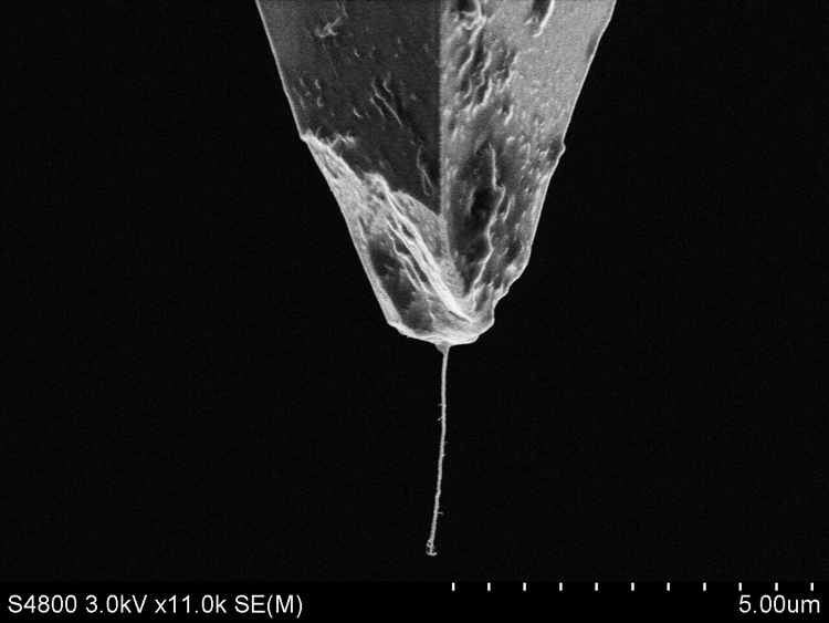
This image shows a carbon nanotube attached to a conventional silicon tip used on an instrument called an atomic force microscope, which is used to measure tiny features on the scale of nanometers. Forces between individual atoms called van der Waals' forces cause the flexible, vibrating probe to stick to the sides of the tiny structures, producing "artifacts," or inaccuracies in the final image. Purdue researchers have shown how to avoid the sticking action and prevent certain artifacts so that nanotubes can be better used in the emerging field of "nanometrology." (Purdue School of Mechanical Engineering). Copyright © Purdue University
|
Researchers attach the tubes to the ends of imaging instruments called atomic force microscopes. Because the tubes are long and slender, their shape is ideal for the emerging field of "nanometrology," which is precisely measuring structures on the scale of nanometers, or billionths of a meter.
Conventional silicon tips used on the microscopes are shaped like inverted traffic cones. They are fine for measuring relatively flat surfaces, but they do not readily penetrate crevices that often exist in tiny devices and structures, said Arvind Raman, an associate professor of mechanical engineering at Purdue. The silicon tips also wear out quickly, reducing image resolution, whereas the carbon nanotubes have been shown to retain their accuracy after many hours of use, said mechanical engineering doctoral student Mark Strus.
But while nanotubes better penetrate the nooks and crannies of nano-structures, the flexible tubes often stick to the sides of these structures due to attractive forces between individual atoms called van der Waals' forces.
"An example I give students is that operating in a nanoscale environment is like having flypaper everywhere because of the attraction of van der Waals' forces," Raman said. "These short-range, inter-atomic forces are very relevant on this size scale because a nanometer is less than 10 atoms wide."
Researchers use nanotubes as probes by inducing a vibration in a portion of the microscope assembly called a microcantilever.
"The microcantilever, which does all of the surface sensing, can be thought of as a very small oscillating diving board on which the silicon tip and nanotube are mounted to the free end," Strus said.
As the microcantilever vibrates, the nanotube tip comes close to the surface but never actually touches the object being imaged. The closer the tip comes to the surface, the more powerful the attractive van der Waals' forces become. The increasing attraction causes changes in the vibration pattern of the oscillating microcantilever, and the changing pattern is carefully monitored to reveal precise changes in contours on the surface of the object, yielding an image.
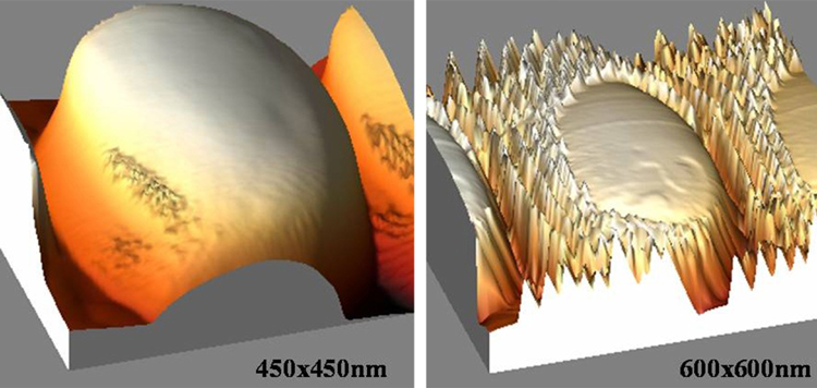
This image shows a comparison between an image taken with a conventional silicon tip (left) and a nanotube, both used on an atomic force microscope to scan the surface of an object to measure tiny contours on the scale of nanometers. While nanotubes are more slender and flexible than the silicon tips, making them ideal to reach into the nooks and crannies of nano-structures, the tubes have a tendency to stick to the sides of the structures because of forces between individual atoms called van der Waals' forces. The sticking action results in "artifacts," or inaccuracies in the final image. The image on the left shows an image taken with a conventional tip, and the other image shows an example of artifacts caused by the sticking action. Purdue researchers have shown how to avoid the sticking action and prevent certain artifacts so that nanotubes can be better used in the emerging field of "nanometrology." (Purdue School of Mechanical Engineering). Copyright © Purdue University
|
The same forces that enable the technology to work, however, also cause the sticking action of the probe. The vibrating tip sticks to the sides of the object being imaged, producing "artifacts," or inaccuracies in the measurements and images.
Strus has led research aimed at oscillating the probes in a manner that prevents nanotubes from sticking to structures, and new findings could lead to more accurate measurements using the slender probes. The journal paper was written by Strus, Raman, C-S Han, senior research manager from the Nanomechanical Systems Research Center at the Korea Institute of Machinery and Materials, and C.V. Nguyen, a research scientists from the NASA Ames Research Center in Moffett Field, Calif.
Methods to precisely measure structures on the scale of nanometers will become essential as nanostructures are used more often in applications such as computer chips, advanced sensors, microscopic machines and the creation of new materials. Precision measurements will be critical for developing new standards needed to properly develop, study and manufacture products based on nanotechnology.
Although some researchers are using nanotube tips in place of conventional silicon tips, the technique is still being perfected and has not yet reached widespread commercial use.
"One of our points in this paper is that you can avoid getting these artifacts if you know how to set the parameters," Strus said. "For example, you can change your set point or your amplitude and still get a good image with your nanotube."
The researchers showed precisely how artifacts are created by the sticking nanotubes, which are about 25 nanometers thick. The researchers also have shown how to avoid these artifacts by adjusting operating parameters of the microscope to prevent the tube from sticking.
One way to decrease the sticking is to increase the amplitude, or how far the probe moves each time it vibrates across the surface. With each oscillation, the tube sweeps close to the surface of the object and then swings in the opposite direction, constantly repeating the motion. As the vibrating probe sticks to the sides of a structure, the microscope's computerized controller pulls the tip farther from the surface. Then, after the tip is pulled away, it starts vibrating normally again, and the controller repositions it closer to the surface, again resulting in the sticking action. This cycle repeats, causing the image artifacts.
The researchers demonstrated how to prevent several specific types of artifacts while using nanotubes to take images of tiny tungsten posts about 100 nanometers in diameter and other nano-structures.
The research was funded by the Centre for Nanomechatronics and Manufacturing in South Korea, and the work is associated with Purdue's Birck Nanotechnology Center, which is part of Discovery Park, the university's hub for interdisciplinary research.
Writer:
Emil Venere, (765) 494-4709, venere@purdue.edu
Sources:
Arvind Raman, (765) 494-5733, raman@ecn.purdue.edu
Mark Strus, (765) 496-6416, mstrus@purdue.edu
Related Web sites:
The journal Nanotechnology
Arvind Raman
Contact:
Purdue University
News Service
400 Centennial Mall Drive, Rm. 324
West Lafayette, IN 47907-2016
(765) 494-2096
fax: (765) 494-0401
purduenews@purdue.edu
Copyright � Purdue University
If you have a comment, please Contact us.
Issuers of news releases, not 7th Wave, Inc. or Nanotechnology Now, are solely responsible for the accuracy of the content.
Bookmark:


| Related News Press |
Nanotubes/Buckyballs/Fullerenes/Nanorods/Nanostrings
![]() Tests find no free-standing nanotubes released from tire tread wear September 8th, 2023
Tests find no free-standing nanotubes released from tire tread wear September 8th, 2023
![]() Detection of bacteria and viruses with fluorescent nanotubes July 21st, 2023
Detection of bacteria and viruses with fluorescent nanotubes July 21st, 2023
Announcements
![]() NRL charters Navy�s quantum inertial navigation path to reduce drift April 5th, 2024
NRL charters Navy�s quantum inertial navigation path to reduce drift April 5th, 2024
![]() Discovery points path to flash-like memory for storing qubits: Rice find could hasten development of nonvolatile quantum memory April 5th, 2024
Discovery points path to flash-like memory for storing qubits: Rice find could hasten development of nonvolatile quantum memory April 5th, 2024
Tools
![]() Ferroelectrically modulate the Fermi level of graphene oxide to enhance SERS response November 3rd, 2023
Ferroelectrically modulate the Fermi level of graphene oxide to enhance SERS response November 3rd, 2023
![]() The USTC realizes In situ electron paramagnetic resonance spectroscopy using single nanodiamond sensors November 3rd, 2023
The USTC realizes In situ electron paramagnetic resonance spectroscopy using single nanodiamond sensors November 3rd, 2023
|
|
||
|
|
||
| The latest news from around the world, FREE | ||
|
|
||
|
|
||
| Premium Products | ||
|
|
||
|
Only the news you want to read!
Learn More |
||
|
|
||
|
Full-service, expert consulting
Learn More |
||
|
|
||