Home > Press > Nano cluster devices announces new nano-patterning technologies
Abstract:
New technologies allow faster and easier patterning of nanodevices
Nano cluster devices announces new nano-patterning technologies
Christchurch, New Zealand | August 07, 2005
Two new technologies for fabricating tiny electronic devices have been unveiled by Christchurch, New Zealand, based Nano Cluster Devices Ltd.
The first technology is a new variation on the techniques used by the semiconductor industry to produce computer chips. Ren� Reichel, a PhD student who played a key role in developing the techniques, said, �Our new technique eliminates one of the processing steps that is currently needed to do lithography.�
The new technology can be used to produce patterns in almost any shape, and has been demonstrated by fabricating a tiny map of New Zealand, as well as electronic devices more than 1000 times smaller than the thickness of a human hair. All of NCD�s technologies are based on the assembly of clusters, which are particles with dimensions of a few billionths of a metre.
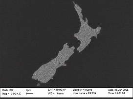
Map of New Zealand produced using NCD�s No-Liftoff LithographyTM technique.
About 100,000 of these maps would fit on the head of a pin.
|
The second technology is an improvement on stencilling techniques that are widely used in industry, but often suffer from problems where the stencils �clog.�
�It�s a bit like spray painting through a stencil, except that we are spraying clusters and not paint,� says Dr Jim Partridge who was the lead researcher on both projects. �By controlling the conditions so that the clusters do not stick to the stencil, we have shown that we can eliminate clogging and make very narrow wires.�
�These are really significant developments,� says NCD Chief Scientist Dr Simon Brown. �These new technologies allow faster and easier patterning of nanodevices, and may provide significant economic and technical advantages over existing technologies used by the semiconductor industry.�
The new technologies were developed by Jim Partridge, Ren� Reichel and David Mackenzie in the Department of Physics and Astronomy at the University of Canterbury on behalf of NCD. NCD has filed patent applications on the new technologies in addition to those for its previously announced methods of self-assembling clusters (or nanoparticles) into nanowires.
Nanotechnology is an emerging field widely seen as having as great an importance as biotechnology and information technology. Nanotechnology will have tremendous impacts in these fields as well as in electronics, medicine and many others. NCD�s self-assembled nanowires could also be used as the key components in transistors or as interconnects between devices on silicon chips. Nanowires therefore have the potential to enable much smaller and faster computers than those possible today.
NCD�s Dr Brown has recently been invited to present at the prestigious NanoCommerce / SEMI NanoForum in Chicago in early November. Last month, NCD�s nanowire technology was showcased to the international semiconductor industry, after selection by a panel of industry experts for the Technology Innovation Showcase (TIS) in conjunction with the SEMICON West conference in San Francisco in July.
About Nano Cluster Devices Ltd.:
Nano Cluster Devices Ltd was formed in early 2003 to commercialize a unique combination of top down and bottom up approaches to nano-technology. The key aspect of the technology is that nano-wires can be self-assembled between electrical contacts without the time consuming and expensive manipulation that typically hinders the production of nano-devices.
Nano Cluster Devices Limited has developed novel methods for taking clusters of atoms and forming them into electrically conducting wires. These wires are so small they can only be seen with the aid of an electron microscope. They have a wide range of applications in many of the world�s multi-billion dollar industries. A comprehensive Patent Portfolio has been established.
For more information visit www.nanoclusterdevices.com
Contact:
Simon Brown
Phone: 03 3642507
Copyright � Nano Cluster Devices Ltd
If you have a comment, please Contact us.
Issuers of news releases, not 7th Wave, Inc. or Nanotechnology Now, are solely responsible for the accuracy of the content.
Bookmark:


| Related News Press |
Chip Technology
![]() Discovery points path to flash-like memory for storing qubits: Rice find could hasten development of nonvolatile quantum memory April 5th, 2024
Discovery points path to flash-like memory for storing qubits: Rice find could hasten development of nonvolatile quantum memory April 5th, 2024
![]() Utilizing palladium for addressing contact issues of buried oxide thin film transistors April 5th, 2024
Utilizing palladium for addressing contact issues of buried oxide thin film transistors April 5th, 2024
![]() HKUST researchers develop new integration technique for efficient coupling of III-V and silicon February 16th, 2024
HKUST researchers develop new integration technique for efficient coupling of III-V and silicon February 16th, 2024
Self Assembly
![]() Liquid crystal templated chiral nanomaterials October 14th, 2022
Liquid crystal templated chiral nanomaterials October 14th, 2022
![]() Nanoclusters self-organize into centimeter-scale hierarchical assemblies April 22nd, 2022
Nanoclusters self-organize into centimeter-scale hierarchical assemblies April 22nd, 2022
![]() Atom by atom: building precise smaller nanoparticles with templates March 4th, 2022
Atom by atom: building precise smaller nanoparticles with templates March 4th, 2022
![]() Nanostructures get complex with electron equivalents: Nanoparticles of two different sizes break away from symmetrical designs January 14th, 2022
Nanostructures get complex with electron equivalents: Nanoparticles of two different sizes break away from symmetrical designs January 14th, 2022
Nanoelectronics
![]() Interdisciplinary: Rice team tackles the future of semiconductors Multiferroics could be the key to ultralow-energy computing October 6th, 2023
Interdisciplinary: Rice team tackles the future of semiconductors Multiferroics could be the key to ultralow-energy computing October 6th, 2023
![]() Key element for a scalable quantum computer: Physicists from Forschungszentrum J�lich and RWTH Aachen University demonstrate electron transport on a quantum chip September 23rd, 2022
Key element for a scalable quantum computer: Physicists from Forschungszentrum J�lich and RWTH Aachen University demonstrate electron transport on a quantum chip September 23rd, 2022
![]() Reduced power consumption in semiconductor devices September 23rd, 2022
Reduced power consumption in semiconductor devices September 23rd, 2022
![]() Atomic level deposition to extend Moore�s law and beyond July 15th, 2022
Atomic level deposition to extend Moore�s law and beyond July 15th, 2022
Announcements
![]() NRL charters Navy�s quantum inertial navigation path to reduce drift April 5th, 2024
NRL charters Navy�s quantum inertial navigation path to reduce drift April 5th, 2024
![]() Discovery points path to flash-like memory for storing qubits: Rice find could hasten development of nonvolatile quantum memory April 5th, 2024
Discovery points path to flash-like memory for storing qubits: Rice find could hasten development of nonvolatile quantum memory April 5th, 2024
|
|
||
|
|
||
| The latest news from around the world, FREE | ||
|
|
||
|
|
||
| Premium Products | ||
|
|
||
|
Only the news you want to read!
Learn More |
||
|
|
||
|
Full-service, expert consulting
Learn More |
||
|
|
||