Home > Press > Gold Nano Anchors Put Nanowires in Their Place
Abstract:
NIST researchers have demonstrated a technique for growing well-formed, single-crystal nanowires
Gold Nano Anchors Put Nanowires in Their Place
Researchers at the National Institute of Standards and Technology (NIST) have demonstrated a technique for growing well-formed, single-crystal nanowires in place�and in a predictable orientation�on a commercially important substrate.
The method uses nanoparticles of gold arranged in rows on a sapphire surface as starting points for growing horizontal semiconductor "wires" only 3 nanometers (nm) in diameter. Other methods produce semiconductor nanowires more than 10 nm in diameter. NIST chemists' work was highlighted in the Oct. 11 issue of Applied Physics Letters.*
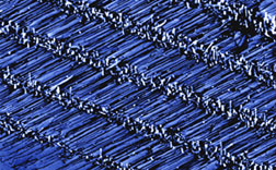
Scanning electron microscope image shows rows of horizontal zinc-oxide nanowires grown on a sapphire surface. The gold nanoparticles are visible on the ends of each row. Click for larger version. Copyright © NIST |
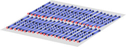
Illustration shows how crystalline zinc oxide nanowires (blue) push "seeds" of gold nanoparticles (red) forward as they grow. Click for larger version. Copyright © NIST |
Part of the vision of nanotechnology is the possibility of building powerful, extraordinarily compact sensors and other devices out of atomic-scale components. So-called �nanowires��long thin crystals of, e.g., a semiconductor� could not only link nanoelectronic devices like conventional wire but also function as devices themselves, tipped with photodetector or light-emitting elements, for example.
An obvious stumbling block is the problem of working with components so small that only the most sophisticated measurement instruments can even track them. To date, the most successful nanowire alignment method involved growing large numbers of the rod-like crystals on a suitable base like blades of grass, shearing them off, mixing them in a solvent, and forcing them to align by either flow or surface confinement on the test substrate to orient most of the crystals in a specific horizontal direction. Further photolithography steps are required to ensure that nanowires are positioned correctly.
In contrast, the NIST technique grows arrays of nanowires made of zinc oxide, a semiconductor widely used in optoelectronics, with precise alignments. The gold "anchors" are placed with a chemical etching step and the orientation of the wires�horizontal, vertical or at a 60 degree angle from the surface�is determined by tweaking the size of the gold particles.
*B. Nikoobakht, C.A. Michaels, S.J. Stranick, M. Vaudin, Applied Physics Letters, Oct. 11, 2004, Vol. 85, Issue 15, pp. 3244-3246.
Media contact:
Michael Baum
michael.baum@nist.gov
(301) 975-2763
Copyright � NIST
If you have a comment, please us.
Issuers of news releases, not 7th Wave, Inc. or Nanotechnology Now, are solely responsible for the accuracy of the content.
Bookmark:


| Related News Press |
Possible Futures
![]() Discovery points path to flash-like memory for storing qubits: Rice find could hasten development of nonvolatile quantum memory April 5th, 2024
Discovery points path to flash-like memory for storing qubits: Rice find could hasten development of nonvolatile quantum memory April 5th, 2024
![]() With VECSELs towards the quantum internet Fraunhofer: IAF achieves record output power with VECSEL for quantum frequency converters April 5th, 2024
With VECSELs towards the quantum internet Fraunhofer: IAF achieves record output power with VECSEL for quantum frequency converters April 5th, 2024
Sensors
Nanoelectronics
![]() Interdisciplinary: Rice team tackles the future of semiconductors Multiferroics could be the key to ultralow-energy computing October 6th, 2023
Interdisciplinary: Rice team tackles the future of semiconductors Multiferroics could be the key to ultralow-energy computing October 6th, 2023
![]() Key element for a scalable quantum computer: Physicists from Forschungszentrum J�lich and RWTH Aachen University demonstrate electron transport on a quantum chip September 23rd, 2022
Key element for a scalable quantum computer: Physicists from Forschungszentrum J�lich and RWTH Aachen University demonstrate electron transport on a quantum chip September 23rd, 2022
![]() Reduced power consumption in semiconductor devices September 23rd, 2022
Reduced power consumption in semiconductor devices September 23rd, 2022
![]() Atomic level deposition to extend Moore�s law and beyond July 15th, 2022
Atomic level deposition to extend Moore�s law and beyond July 15th, 2022
Discoveries
![]() Chemical reactions can scramble quantum information as well as black holes April 5th, 2024
Chemical reactions can scramble quantum information as well as black holes April 5th, 2024
![]() New micromaterial releases nanoparticles that selectively destroy cancer cells April 5th, 2024
New micromaterial releases nanoparticles that selectively destroy cancer cells April 5th, 2024
![]() Utilizing palladium for addressing contact issues of buried oxide thin film transistors April 5th, 2024
Utilizing palladium for addressing contact issues of buried oxide thin film transistors April 5th, 2024
Announcements
![]() NRL charters Navy�s quantum inertial navigation path to reduce drift April 5th, 2024
NRL charters Navy�s quantum inertial navigation path to reduce drift April 5th, 2024
![]() Discovery points path to flash-like memory for storing qubits: Rice find could hasten development of nonvolatile quantum memory April 5th, 2024
Discovery points path to flash-like memory for storing qubits: Rice find could hasten development of nonvolatile quantum memory April 5th, 2024
|
|
||
|
|
||
| The latest news from around the world, FREE | ||
|
|
||
|
|
||
| Premium Products | ||
|
|
||
|
Only the news you want to read!
Learn More |
||
|
|
||
|
Full-service, expert consulting
Learn More |
||
|
|
||